
Fabrication method for patterning sapphire light giving-out surface of LED flip chip

A technology of flip chip and manufacturing method, which is applied in the direction of electrical components, circuits, semiconductor devices, etc., can solve problems such as difficult application of nanoimprinting technology, sapphire fragmentation, etc., and achieve improved light extraction efficiency, easy operation, and tolerance high effect

Inactive Publication Date: 2018-03-30
JIANGSU XINGUANGLIAN SEMICON
View PDF19 Cites 9 Cited by
  • Summary
  • Abstract
  • Description
  • Claims
  • Application Information

AI Technical Summary

Problems solved by technology

For the flip-chip sapphire light-emitting surface in this case, since the sapphire is very thin, only 150 microns thick, using imprinting technology under this thickness will easily cause sapphire fragmentation, and nano-imprinting technology is also difficult to apply

Method used


Image

  • Fabrication method for patterning sapphire light giving-out surface of LED flip chip
  • Fabrication method for patterning sapphire light giving-out surface of LED flip chip
  • Fabrication method for patterning sapphire light giving-out surface of LED flip chip

Examples


Embodiment Construction

[0026] The present invention will be further described below in conjunction with specific drawings and embodiments.

[0027] For the patterning of the sapphire light-emitting surface of LED flip chips, after research, laser direct writing is another feasible lithography method. Its working principle is to control the high-precision laser beam scanning by computer, and directly expose and write Arbitrary graphics designed, so that the design graphics can be directly transferred to the substrate. Laser direct writing lithography, no mask plate required, high graphics resolution, fast lithography writing efficiency, high repeat alignment accuracy, adaptive to changes in the environment and substrate thickness, and easy to operate.

[0028] The specific steps of this process method are as follows:

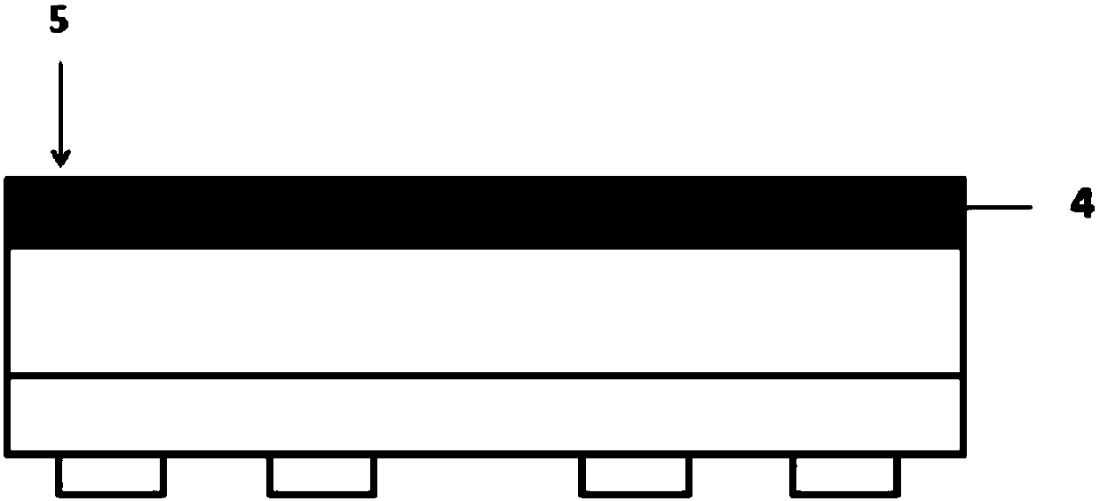
[0029] Step S1, such as figure 2 As shown, the LED chip front-end process is completed by the normal flip-chip process until the sapphire substrate thinning and polishing process is...


PUM


Abstract

The invention provides a fabrication method for patterning a sapphire light giving-out surface of an LED flip chip. The fabrication method comprises the following steps of S1, completing fabrication of a front process of the LED chip by a normal flip chip process until a sapphire substrate thinning and polishing process is completed, wherein the structure comprises a thinned sapphire substrate, aGaN epitaxial layer and an electrode of the flip chip from top to bottom; S2, coating photoresist on a surface of a back surface of the sapphire substrate, and completing a photoetching process by laser direct writing exposure; S3, forming a preset photoresist pattern on a surface of the back surface of the sapphire substrate after exposure and developing, and etching the surface of the back surface of the sapphire substrate by an ICP dry-etching method; and S4, forming a pattern on the surface of the back surface of the sapphire substrate after the resided photoresist is removed.

Description

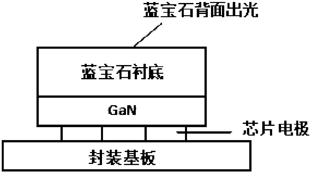
technical field [0001] The invention relates to an LED chip process, in particular to a process for patterning the sapphire light-emitting surface of an LED flip-chip. Background technique [0002] In recent years, light-emitting diode (LED) has become the most important light source technology, among which LED flip-chip technology has become one of the hot spots. Compared with front-mounted chips, LED flip-chip products have the characteristics of low voltage, high brightness, high reliability, and high saturation current density, and have excellent development prospects. [0003] A typical LED flip-chip schematic diagram is shown in figure 1 . Usually the chip structure includes a sapphire substrate, a gallium nitride (GaN) layer and two chip electrodes respectively. When flip-chip is used, the front is facing down, and the two chip electrodes are connected to the packaging substrate below. After the light is emitted from the GaN layer, it exits from the back of the sap...

Claims


Application Information

Patent Timeline
Patent Type & Authority Applications(China)
IPC IPC(8): H01L33/00H01L33/20
CPCH01L33/007H01L33/20
Inventor 华斌张秀敏闫晓密黄慧诗
Owner JIANGSU XINGUANGLIAN SEMICON
Learn More