All-inorganic light-emitting device based on perovskite thin film and preparation method thereof

A light-emitting device, perovskite technology, applied in the direction of semiconductor devices, nanotechnology for materials and surface science, electrical components, etc., to achieve the effect of high luminous purity, stable performance, and simple structure

Active Publication Date: 2018-03-30
上海镓旦电子信息有限公司
View PDF3 Cites 9 Cited by
  • Summary
  • Abstract
  • Description
  • Claims
  • Application Information

AI Technical Summary

Problems solved by technology

[0005] The purpose of the present invention is to provide an all-inorganic light-emitting device based on a perovskite film and its preparation method in view of the deficiencies and problems in the existing preparation of light-emitting devices

Method used


Image

  • All-inorganic light-emitting device based on perovskite thin film and preparation method thereof
  • All-inorganic light-emitting device based on perovskite thin film and preparation method thereof
  • All-inorganic light-emitting device based on perovskite thin film and preparation method thereof

Examples


Embodiment 1

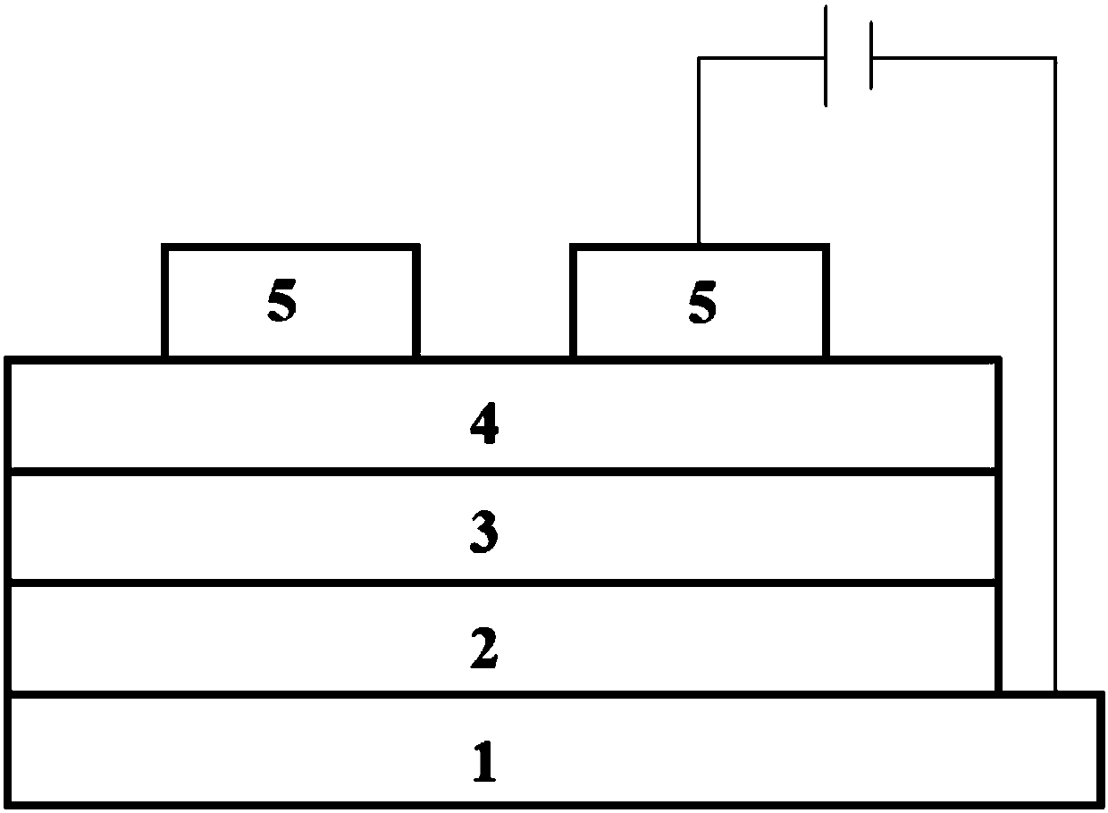
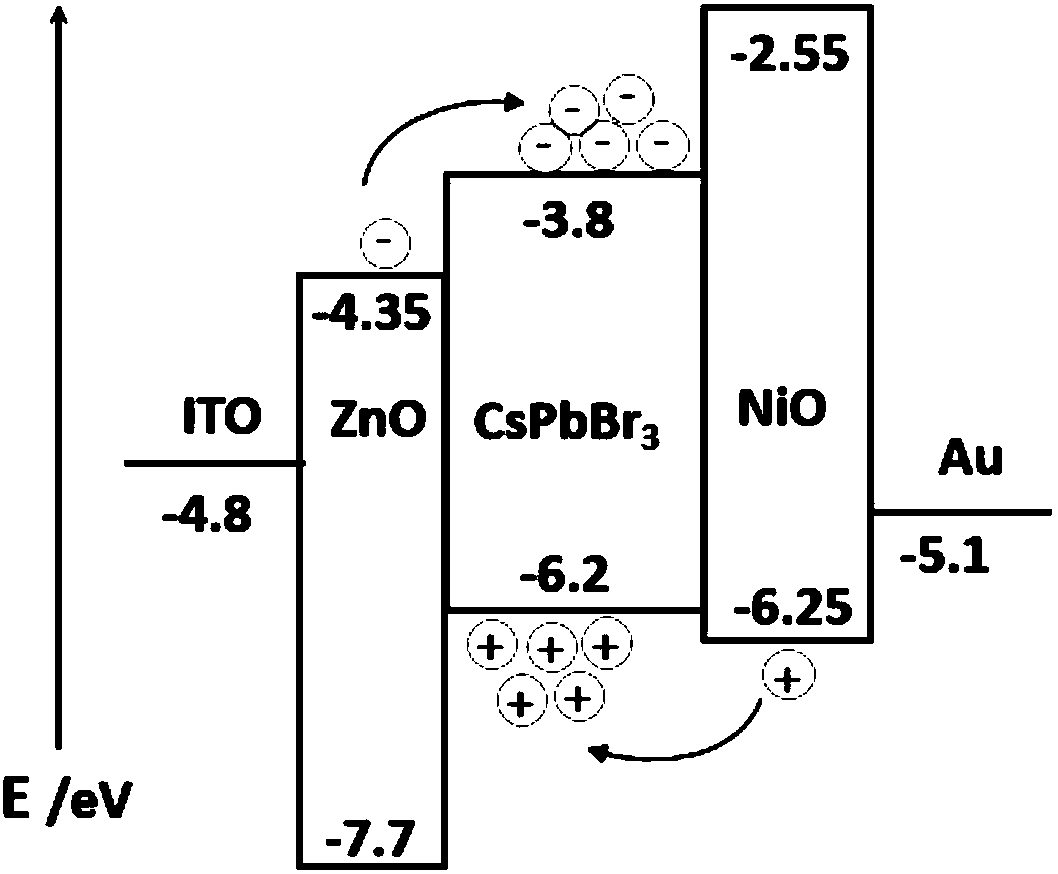
[0026] (1) Use toluene, acetone, ethanol, and deionized water in sequence to ultrasonically clean the ITO glass substrate for 5 minutes, and then dry the substrate with a nitrogen gun for later use;

[0027] (2) Deposit the ZnO electron transport layer 2 on the ITO conductive film of the cleaned ITO glass substrate by magnetron sputtering. The target used for sputtering is a ZnO target with a diameter of 46 mm and a copper back target of 50 mm, Ar and O 2 The gas flow rate is 40sccm, the reaction chamber pressure is set to 20mTorr, the sputtering power of the RF source is set to 70W, the target speed is 25 rpm, and the final deposition thickness is 50nm;

[0028] (3) Depositing PbBr on the ZnO electron transport layer by thermal evaporation 2 layer, and then soak the obtained device into a saturated ethanol solution of CsBr for 15 minutes, and anneal at 85°C for 25 minutes after the reaction is complete, and prepare the inorganic perovskite CsPbBr 3 Thin film light emitting ...

Embodiment 2

[0033] (1) Use toluene, acetone, ethanol, and deionized water to clean the ITO glass substrate ultrasonically for 5 minutes, and then dry the substrate with a nitrogen gun for later use.

[0034] (2) Deposit the ZnO electron transport layer 2 on the ITO conductive film of the cleaned ITO glass substrate by magnetron sputtering. The target used for sputtering is a ZnO target with a diameter of 46 mm and a copper back target of 50 mm, Ar and O 2 The gas flow rate is 40sccm, the reaction chamber pressure is set to 20mTorr, the sputtering power of the RF source is set to 70W, the target speed is 25 rpm, and the final deposition thickness is 50nm;

[0035] (3) Depositing PbI on the ZnO electron transport layer by thermal evaporation 2layer, and then soak the obtained device in a saturated ethanol solution of CsI for 15 minutes, and anneal at 80-90°C for 25 minutes after the reaction is complete, to prepare the inorganic perovskite CsPbI 3 Thin film light emitting layer. Thermall...


PUM

PropertyMeasurementUnit
thicknessaaaaaaaaaa
thicknessaaaaaaaaaa
thicknessaaaaaaaaaa

Abstract

The invention provides an all-inorganic light-emitting device based on a perovskite thin film and a preparation method thereof, and belongs to the technical field of semiconductor light-emitting devices. The all-inorganic light-emitting device is composed of an ITO glass substrate, a ZnO electron transmission layer, an inorganic perovskite CsPbX3 thin film light-emitting layer, an NiO hole transmission layer and an Au and Al anode electrode layer which are laminated in turn from the bottom to the top, wherein the ZnO electron transmission layer is prepared on the ITO conductive film of the ITOglass substrate, the ITO conductive film acts as a cathode electrode layer, and X is Cl, Br or I element. The surface of the perovskite CsPbX3 thin film is flat without pinhole, and the grain size issmall and efficient radiation composite luminescence can be easily realized so that the luminescence purity is high and the luminescence range is adjustable by adjusting and controlling the doping proportion of the halogen atoms. The inorganic material ZnO/NiO of stable property is used as the electron/hole transmission layer of the device so that the requirement of the working environment of thedevice is ensured to be low and the performance is stable.

Description

technical field [0001] The invention belongs to the technical field of semiconductor light-emitting devices, and in particular relates to an all-inorganic light-emitting device based on a perovskite thin film and a preparation method thereof. Background technique [0002] At present, most commercial light-emitting devices in the market are made of gallium nitride materials, which have done a good job in terms of brightness and efficiency, but there are still some problems, such as high requirements for the substrate (the substrate and the epitaxial layer need to be relatively low). The lattice mismatch and thermal mismatch) and the defect tolerance is low, the cost is relatively high; and full spectral coverage cannot be achieved. However, light-emitting devices based on perovskite materials can solve these problems. The perovskite material is an ABX 3 Type of structural material, the A site is generally metal cations such as rare earth or alkaline earth elements, and the ...

Claims


Application Information

Patent Timeline
Patent Type & Authority Applications(China)
IPC IPC(8): H01L33/00H01L33/02H01L33/26B82Y30/00
CPCB82Y30/00H01L33/0012H01L33/005H01L33/02H01L33/26
Inventor 张宝林庄仕伟张源涛董鑫马雪
Owner 上海镓旦电子信息有限公司
Why Eureka
Try Eureka