Array target of X-ray source for electron beam scanning CT and manufacturing method of array target

A technology of electron beam scanning and manufacturing method, applied in parts of X-ray tube, X-ray/γ-ray/particle irradiation therapy, etc. Charge-discharge effect, increase thermal conductivity, avoid the effect of charge effect

Active Publication Date: 2018-04-06
CHINA ELECTRONIC TECH GRP CORP NO 38 RES INST
View PDF6 Cites 5 Cited by
  • Summary
  • Abstract
  • Description
  • Claims
  • Application Information

AI Technical Summary

Problems solved by technology

The energy density of the focused electron beam is high, and more than 99% of it is converted into heat. In the area where the electron beam bombards the anode target, the temperature gradient can be as high as 10 5 ℃ / mm, the local temperature rise is extremely high, and the point-like tandem structure targets are independent and have no contact around them, so the heat cannot be transferred in time, and it is easy to cause the target to be burned
[0008] In addition, the conductivity of the above-mentioned point-like serial structure targets will have a serious impact on the X-ray emission.
There is no contact around the point-like serial structure target, only the bottom surface is in contact with the target base. If the target base is made of materials with poor conductivity such as diamond, it will cause charge and discharge effects. When the incident electron beam bombards the conductive anode target, the surface of the anode target will It is easy to cause charge accumulation, resulting in a drop in target current

Method used


Image

  • Array target of X-ray source for electron beam scanning CT and manufacturing method of array target
  • Array target of X-ray source for electron beam scanning CT and manufacturing method of array target
  • Array target of X-ray source for electron beam scanning CT and manufacturing method of array target

Examples


Embodiment Construction

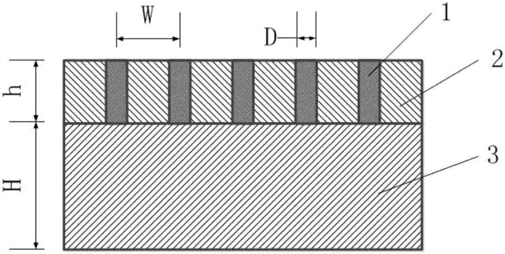
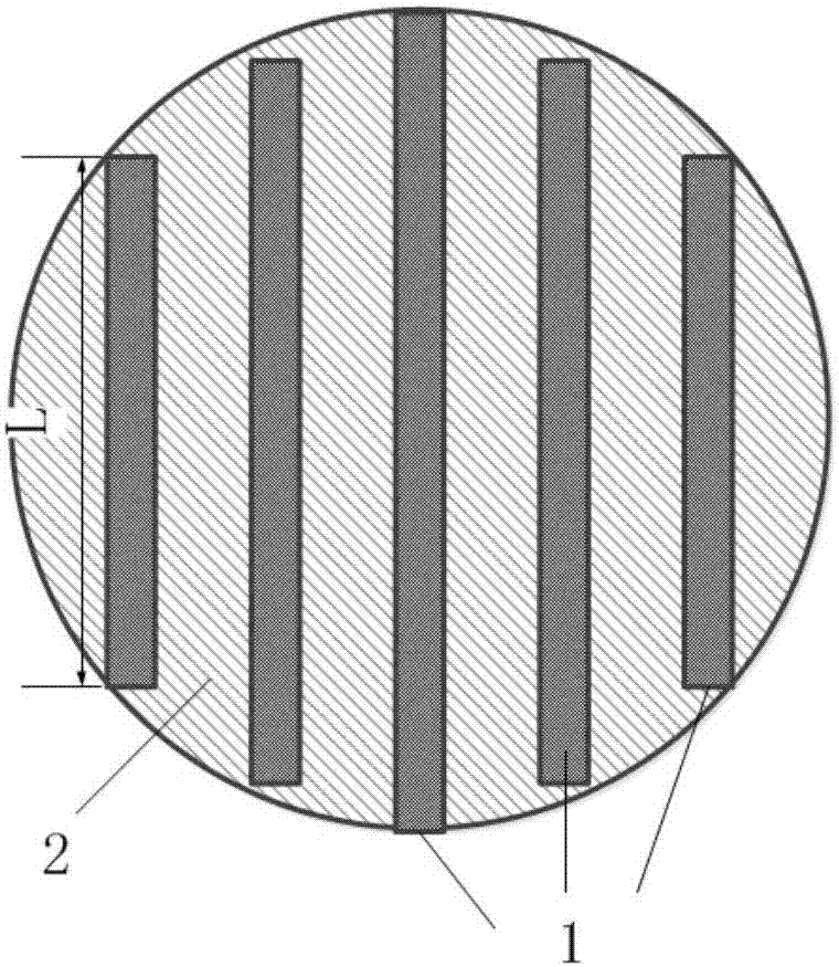
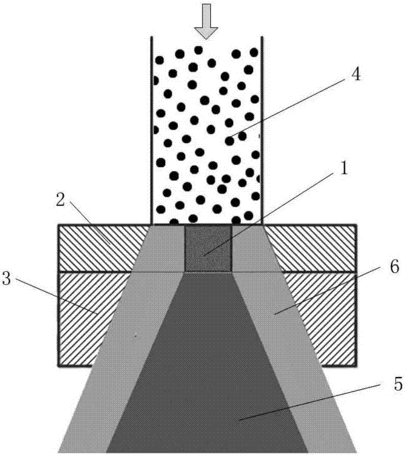
[0036] Such as figure 1 , figure 2 with image 3 As shown, an array target for an X-ray source of electron beam scanning CT, including a linear array target position, an embedding layer 2 and a target base 3;

[0037] The linear array target site includes at least one individual target site 1, the individual target site 1 is in the shape of a line, 0.5 to 10 μm deep into the embedding layer, and the two ends of the target site 1 extend to the embedding layer The edge of layer 2, its function is: the metal target is connected with the metal sealing part on the edge of the embedded layer to form a conductive channel, which is beneficial to charge transfer and avoids the charge accumulation (charging effect) caused by the electron beam. The width of the target position 1 / 2 to 2 / 3 of the diameter of the electron beam; several target positions 1 form a linear array target position;

[0038] The embedding layer 2 is used to configure the target site 1;

[0039] The target base ...


PUM


Abstract

The invention relates to an array target of an X-ray source for electron beam scanning CT. The array target includes a linear array target, an embedding layer, and a target base; the linear array target comprises at least one individual target site; the individual target sites is in the shape of a line and go deep into the embedding layer by 0.5 to 10 microns; two ends of each target site extend to the edges of the embedding layer; the width of the target sites is smaller than or equal to the diameter of an electron beam, preferably, is the half peak width of the beam current density of the electron beam, and can be approximated to 1/2 to 2/3 of the diameter of the electron beam; each gap between the target sites is equal to or greater than the diameter of the electron beam; the embeddinglayer is used for configuring the target sites; the target base is disposed at the bottoms of the embedding layer and the target sites; and the thickness of the target base ranges from 20 to 300 microns.

Description

technical field [0001] The invention relates to an array target for an X-ray source of electron beam scanning CT and a manufacturing method thereof. Background technique [0002] Conventional CT systems use a single-beam X-ray source structure, that is, a single electron emission source and a corresponding single anode target. The electron emission source generates electrons, and the electron beam is accelerated under an electric field and bombards the anode target to generate a single X-ray focus. Shoots a single beam of X-rays. The X-ray source rotates mechanically around the scanned object to collect reconstructed projection images from different viewing angles. In this scanning mode, the limited mechanical rotation speed limits the data acquisition rate of the CT system and complicates the system design. [0003] In the current electron beam scanning CT detection technology, the electron emission source corresponds to a flat anode target, and the electron beam emitted ...

Claims


Application Information

Patent Timeline
Patent Type & Authority Applications(China)
IPC IPC(8): H01J35/02A61N5/10
CPCA61N5/10H01J35/02
Inventor 郑磊刘华荣王俊听李艺晶罗婷婷
Owner CHINA ELECTRONIC TECH GRP CORP NO 38 RES INST
Why Eureka
Try Eureka