Preparation method of enhanced GaN HEMT

An enhanced and p-type technology, applied in semiconductor/solid-state device manufacturing, electrical components, circuits, etc., can solve problems such as leakage, damage interface, and affect device stability, so as to reduce gate leakage, reduce interface state, The effect of avoiding damage

Inactive Publication Date: 2018-04-06
INST OF SEMICONDUCTORS - CHINESE ACAD OF SCI
View PDF4 Cites 11 Cited by
  • Summary
  • Abstract
  • Description
  • Claims
  • Application Information

AI Technical Summary

Problems solved by technology

During the etching and etching process of these two methods, the plasma will damage the interface and affect the stability of the device; the third method for the p-type gate is to perform selective secondary epitaxy on the gate region

Method used


Image

  • Preparation method of enhanced GaN HEMT
  • Preparation method of enhanced GaN HEMT
  • Preparation method of enhanced GaN HEMT

Examples


Embodiment Construction

[0027] The technical solutions in the embodiments of the present invention are clearly and completely described below in conjunction with the accompanying drawings in the embodiments of the present invention. Obviously, the described embodiments are only part of the embodiments of the present invention, not all of them. Those skilled in the art can make similar extensions without departing from the connotation of the present invention, so the present invention is not limited by the specific embodiments disclosed below.

[0028] see figure 1 , Figure 2-Figure 9 As shown, according to the general inventive concept of the present invention, a method for preparing an enhanced GaN HEMT is provided, comprising the following steps:

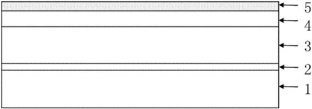
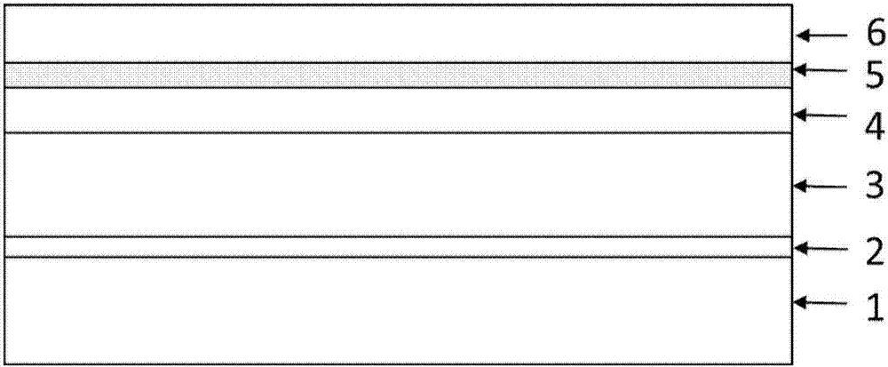
[0029] Step 1: Epitaxial buffer layer 2, channel layer 3, barrier layer 4 and p-type cap layer 5 are sequentially epitaxial on substrate 1 by metalorganic chemical vapor deposition, and the material of substrate 1 is Si, sapphire, SiC or GaN, the buff...


PUM

PropertyMeasurementUnit
Thicknessaaaaaaaaaa
Thicknessaaaaaaaaaa
Thicknessaaaaaaaaaa

Abstract

The invention discloses a preparation method of an enhanced GaN HEMT, comprising the following steps: epitaxially forming a buffer layer, a channel layer, a barrier layer and a p type cap layer in sequence on a substrate through a metal-organic chemical vapor deposition method; preparing a mask layer on the p type cap layer; patterning the mask layer, exposing the p type cap layer of a grid regionpart and then forming a sample; epitaxially forming a p type layer on the exposed p type cap layer of the sample to form a p type grid, namely, epitaxially forming the p type grid in a selected region for the second time; removing the mask layer; etching down to the inside of the channel layer at two sides of the p type cap layer, constructing a table at the two sides of the channel layer and forming table isolation; preparing a source electrode and a drain electrode on the p type cap layer at two sides of the p type grid, and annealing; preparing a grid electrode on the p type grid and forming a device; preparing a passivation layer on the device, wherein the thickness of the passivation layer is higher than the p type grid, and opening the passivation layer of a region of the source electrode, the drain electrode and the grid electrode, namely, exposing the source electrode, the drain electrode and the grid electrode, thereby completing preparation.

Description

technical field [0001] The invention belongs to the technical field of semiconductors, in particular to a method for preparing an enhanced high electron mobility transistor and a semiconductor device including the transistor. Background technique [0002] GaN-based power electronic devices have attracted a lot of attention in recent years. GaN materials can form heterojunction structures with AlGaN, InGaN and other materials. Due to the spontaneous polarization and piezoelectric polarization effects of the barrier layer materials, a high concentration of two-dimensional electron gas (2DEG) will be formed at the heterojunction interface. Due to the advantages of GaN materials such as large band gap, high electron mobility, high electron saturation velocity, and large breakdown field strength, GaN HEMTs have become a research hotspot in the field of microwave power and circuits in the past decade. [0003] Although GaN HEMT has many advantages, it also encounters many proble...

Claims


Application Information

Patent Timeline
IPC IPC(8): H01L29/778H01L21/336
CPCH01L29/66462H01L29/778
Inventor 张韵杨秀霞张连程哲
Owner INST OF SEMICONDUCTORS - CHINESE ACAD OF SCI
Why Eureka
Try Eureka