MEMS piezoresistance type two-axis acceleration sensor chip and preparing method thereof

A sensor chip, shaft acceleration technology, applied in the direction of acceleration measurement using inertial force, can solve the problems affecting the improvement of acceleration sensors, and achieve the effect of improving sensitivity and resonant frequency and improving performance

Active Publication Date: 2018-04-13
XI AN JIAOTONG UNIV
View PDF9 Cites 17 Cited by
  • Summary
  • Abstract
  • Description
  • Claims
  • Application Information

AI Technical Summary

Problems solved by technology

Therefore, there is a mutual restriction relationship between the natural frequency and the sensitivity, which affects the further improvement of the acceleration sensor.

Method used


Image

  • MEMS piezoresistance type two-axis acceleration sensor chip and preparing method thereof
  • MEMS piezoresistance type two-axis acceleration sensor chip and preparing method thereof
  • MEMS piezoresistance type two-axis acceleration sensor chip and preparing method thereof

Examples


preparation example Construction

[0054] Prepare the preparation method of MEMS piezoresistive two-axis acceleration sensor chip of the present invention, comprise the following steps (as Image 6 ):

[0055] Step 1, performing double-sided oxidation on the SOI silicon wafer, so that both the front and back sides of the SOI silicon wafer generate a thermal oxygen silicon dioxide layer 9;

[0056] Step 2, etch the front side of the SOI silicon wafer processed in step 1, etch away the thermal oxygen silicon dioxide layer 9 in the corresponding area of ​​the sensitive beam 5, exposing the device layer 10 of the SOI silicon wafer, and then on the exposed device layer 10 is lightly doped with boron ions, and the lightly doped region of boron ions is used as the varistor strip of the sensitive beam 5;

[0057] Step 3, making a layer of silicon dioxide film 14 on the front side of the SOI silicon wafer processed in step 2;

[0058] Step 4, and then etch the front side of the SOI silicon wafer processed in step 3, e...

Embodiment

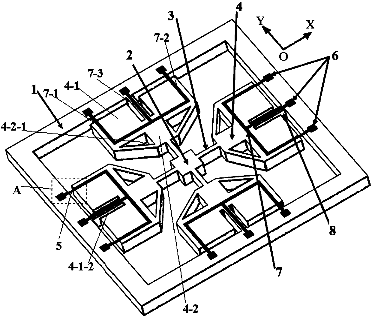
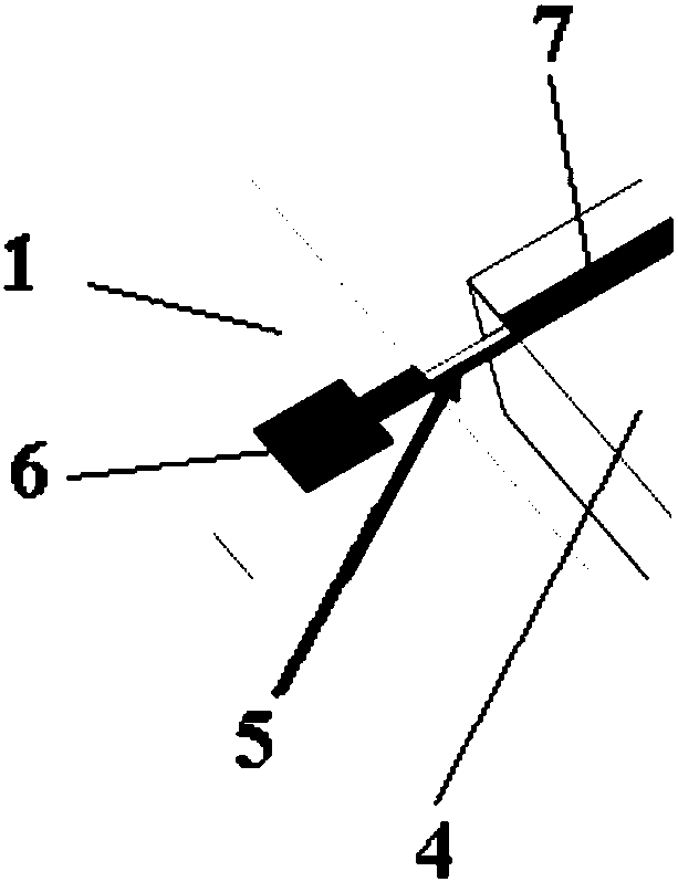
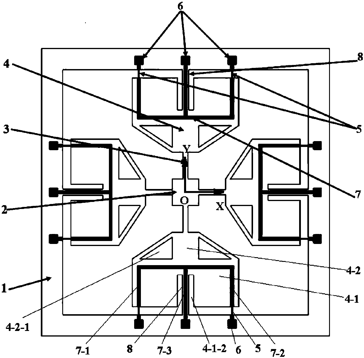
[0071] As a preferred embodiment of the present invention, the acceleration sensor chip of this embodiment consists of four identical substructures, each of which consists of a mass block 4, two sensitive beams 5, an inner support beam 3 and an outer The entire structure formed by connecting the support beams 8, and the pads and metal leads 7 provided on the structure, set the two substructures opposite to the fixed island 2 among the four substructures as a group, and the two groups of substructures form a single axis For the complete structure of the acceleration sensor, the piezoresistor strips on the four sensitive beams 5 of each group are connected through metal leads 7 and six metal pads 6, and form a semi-open-loop Wheatstone full-bridge circuit.

[0072] The sensor chip is prepared using N-type (100) crystal plane SOI silicon wafers. Since the piezoresistive coefficients of [011] and [0ī1] crystal directions are the largest on the (100) crystal plane of silicon, it is ...


PUM

PropertyMeasurementUnit
Thicknessaaaaaaaaaa
Resistivityaaaaaaaaaa
Thicknessaaaaaaaaaa

Abstract

The invention discloses an MEMS piezoresistance type two-axis acceleration sensor chip and a preparing method thereof. The MEMS piezoresistance type two-axis acceleration sensor chip comprises four sets of same sub-structures. The four sub-structures are uniformly distributed at the periphery of a fixed island. The fixed island is connected with a mass block through an inner supporting beam. The mass block is connected with an outer frame through an outer supporting beam. Sensitive beams are symmetrically distributed at two sides of the outer supporting beam. One end of the sensitive beam is connected with one end of the mass block, and the other end of the sensitive beam is connected with the outer frame. The two sub-structures which face each other relative to the fixed island form a set, thereby forming a whole working structure for measuring one acceleration direction, thereby respectively measuring the accelerations in an X-axis and a Y-axis. The two sensitive beams of each sub-structure are respectively provided with a pressure-sensitive resistor and are connected with a pad through metal leads, thereby forming a semi-open-ring Wheatstone full-bridge circuit. The sensor chipcan realize separated measurement of the accelerations below 200g in two axes. The natural frequency of the MEMS piezoresistance type two-axis acceleration sensor reaches above 20kHz, and the sensitivity is higher than 0.5mB / g / 3V. Furthermore the MEMS piezoresistance type two-axis acceleration sensor chip has relatively high resonant frequency and high sensitivity.

Description

technical field [0001] The invention belongs to the field of measurement of micromechanical electronic sensors, and in particular relates to a MEMS piezoresistive two-axis acceleration sensor chip and a preparation method thereof. Background technique [0002] Vibration exists widely in people's daily life and industrial production. The most common way to measure vibration signals is to measure acceleration signals. Vibration acceleration sensors are widely used in industrial control, automotive monitoring, environmental monitoring, consumer electronics and military, etc. It is used to meet the measurement requirements of vibration signals and shock signals in different fields. However, the bulky traditional sensors have become increasingly difficult to meet the actual application requirements in various fields. With the rise of Micro Electro Mechanical Systems (MEMS), acceleration sensors are becoming more and more miniaturized. [0003] There are many measurement principl...

Claims


Application Information

Patent Timeline
IPC IPC(8): G01P15/12
Inventor 蒋维乐于明智赵立波贾琛李支康王久洪赵玉龙蒋庄德
Owner XI AN JIAOTONG UNIV
Why Eureka
Try Eureka