Shallow buried high-voltage Schottky rectifier and manufacturing method thereof
A rectifier, Schottky barrier layer technology, applied in semiconductor/solid-state device manufacturing, semiconductor devices, electrical components, etc., can solve problems such as large leakage current, achieve low leakage current, high breakdown voltage, low forward The effect of pressure drop
- Summary
- Abstract
- Description
- Claims
- Application Information
AI Technical Summary
Problems solved by technology
Method used
Image
Examples
Embodiment 1
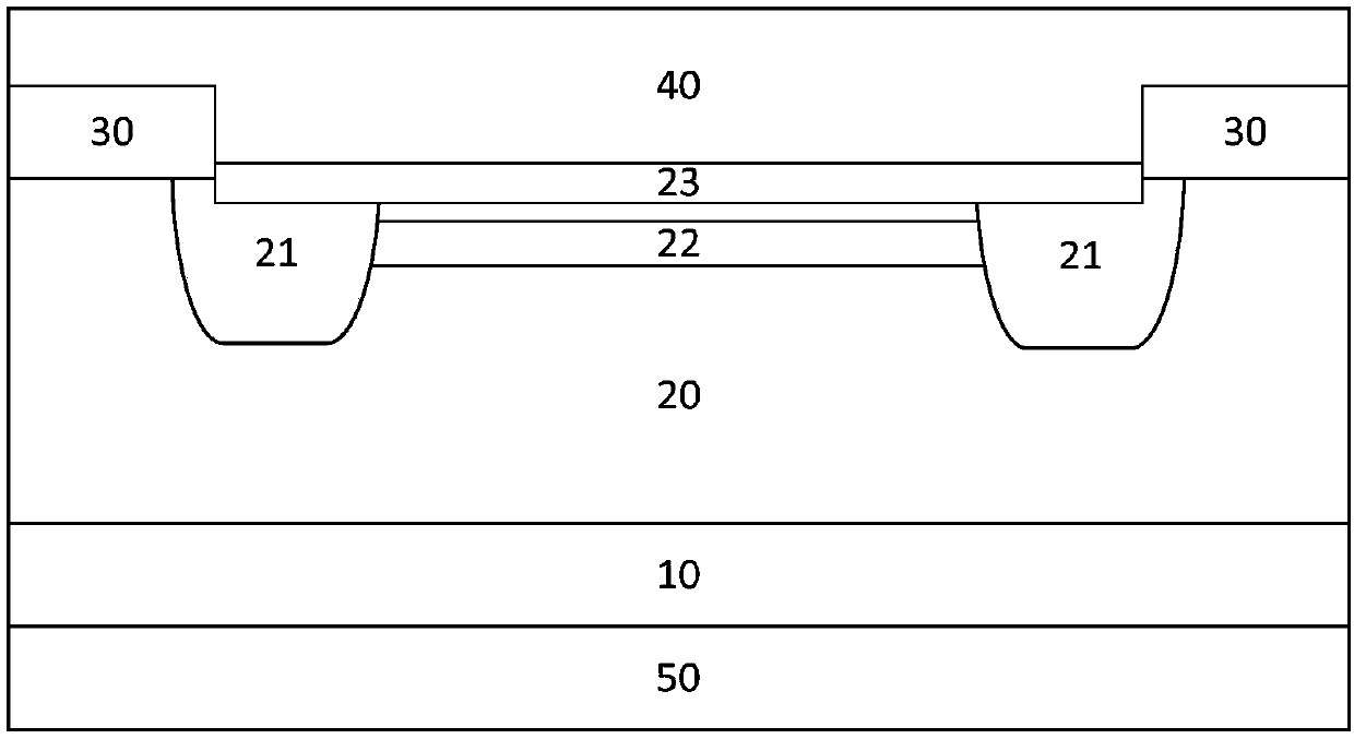
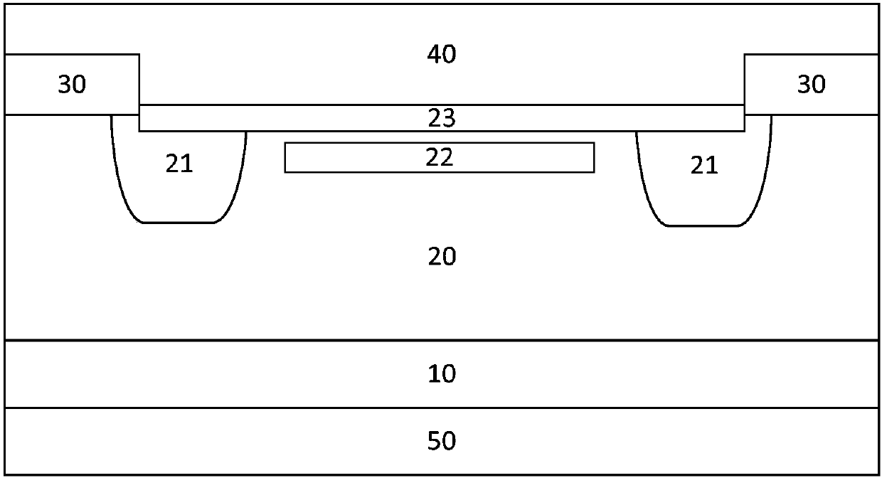
[0037] A shallow-buried high-voltage Schottky rectifier, characterized in that it includes a heavily doped first conductivity type substrate layer 10, a lightly doped first conductivity type epitaxial layer 20, a second conductivity type guard ring region 21, a first conductivity type Type shallow buried layer 22 , Schottky barrier layer 23 , field dielectric layer 30 , anode metal layer 40 and cathode metal layer 50 .
[0038] The heavily doped first conductive type substrate layer 10 covers the cathode metal layer 50 .
[0039] The lightly doped first conductive type epitaxial layer 20 covers the heavily doped first conductive type substrate layer 10 .
[0040] The guard ring region 21 of the second conductivity type covers part of the surface of the epitaxial layer 20 of the lightly doped first conductivity type. The guard ring region 21 of the second conductivity type is a closed ring structure. The middle area surrounded by the ring is the active area.
[0041] The sha...
Embodiment 2
[0046] A method for manufacturing a shallow-buried high-voltage Schottky rectifier, characterized in that it comprises the following steps:
[0047] 1) Covering the lightly doped first conductivity type epitaxial layer 20 on the heavily doped first conductivity type substrate layer 10 .
[0048] 2) Covering the field dielectric layer 30 on the lightly doped epitaxial layer 20 of the first conductivity type.
[0049] 3) Forming a guard ring region 21 of the second conductivity type in a closed ring structure by using the first mask layer. Its annular surrounding part is the active area.
[0050] 4) Etching the field dielectric layer 30 above the active region by using the second mask layer.
[0051] 5) Impurities of the first conductivity type are implanted with high energy into the active region or part of the active region, and the shallow buried layer 22 of the first conductivity type is formed after rapid annealing.
[0052] 6) Covering the Schottky barrier layer 23 on a...
Embodiment 3
[0064] The shallow-buried high-voltage Schottky rectifier, ie, the new device 1, was fabricated using the fabrication method in Example 2. Wherein, the first conductivity type is N type, and the second conductivity type is P type.
[0065] Such as figure 1 As shown, the shallow-buried high-voltage Schottky rectifier produced in this embodiment is characterized in that it includes an N+ type substrate layer 10, an N-type epitaxial layer 20, a P-type guard ring region 21, an N-type shallow buried layer 22, and a Schottky rectifier. Base barrier layer 23 , field dielectric layer 30 , anode metal layer 40 and cathode metal layer 50 .
[0066] The N-type epitaxial layer 20 covers the N+ type substrate layer 10 . The N+ type substrate layer 10 is an arsenic impurity substrate with a doping concentration above the 19th power. The N-type epitaxial layer 20 has an impurity concentration of 2×10 15 cm -3 Phosphorous impurity epitaxial layer.
[0067] The P-type guard ring region 2...
PUM
 Abstract
Description
Claims
Application Information
 - R&D
- Intellectual Property
- Life Sciences
- Materials
- Tech Scout
- Unparalleled Data Quality
- Higher Quality Content
- 60% Fewer Hallucinations
Browse by: Latest US Patents, China's latest patents, Technical Efficacy Thesaurus, Application Domain, Technology Topic, Popular Technical Reports.
© 2025 PatSnap. All rights reserved.Legal|Privacy policy|Modern Slavery Act Transparency Statement|Sitemap|About US| Contact US: help@patsnap.com


