A reconfigurable device with magnetron function based on plasma/dielectric multilayer structure

A plasma layer, plasma technology, applied in the direction of waveguide type devices, electrical components, antennas, etc., can solve the problem of difficult miniaturization of devices and flexible dynamic regulation of frequency, increase the cost of devices, electromagnetic compatibility, and difficult to achieve operating frequency. Tunable and other issues, to achieve the effect of popular processing, flexible design and easy processing

Active Publication Date: 2021-03-23
NANJING UNIV OF POSTS & TELECOMM
View PDF2 Cites 0 Cited by
  • Summary
  • Abstract
  • Description
  • Claims
  • Application Information

AI Technical Summary

Problems solved by technology

The biggest disadvantage of the modification method is that when each functional device is switched, additional control circuits and modules have to be introduced, which not only increases the cost of the device but also brings unavoidable electromagnetic compatibility problems
The problems faced by the existing technology also include that it is difficult to achieve tunability in the working frequency. If the tunable working frequency is to be realized, lumped components have to be added, such as: transformer diodes, transistors and variable capacitors, etc.
These devices have to add additional feed circuits, and it is difficult to make the entire device miniaturized and flexibly adjust the frequency dynamically
There is also a fatal shortcoming in the prior art: the working bandwidth is narrow

Method used


Image

  • A reconfigurable device with magnetron function based on plasma/dielectric multilayer structure
  • A reconfigurable device with magnetron function based on plasma/dielectric multilayer structure
  • A reconfigurable device with magnetron function based on plasma/dielectric multilayer structure

Examples


Embodiment 1

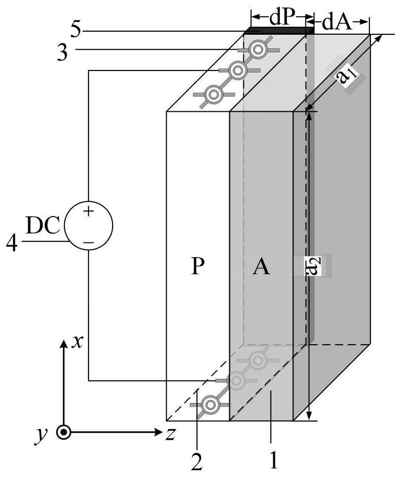
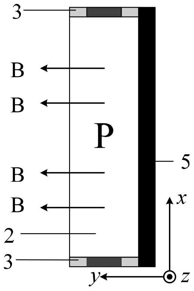
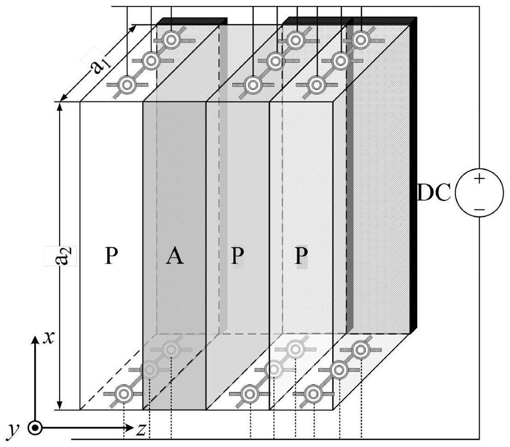
[0042] like figure 1 As shown in FIG. 3 , it is a reconfigurable device with magnetron function based on a plasma / dielectric multilayer structure according to an embodiment. figure 1 For the introduced nested fractal initial sequence S 0 Schematic diagram of the structure; figure 2 The initial sequence of nested fractals introduced for Schematic diagram of the structure; Figure 3a and Figure 3b They are structural schematic diagrams of fractal orders n=1 and n=2, respectively. Figure 4 Schematic diagram of the structure of the metal electrode array used for plasmospheric excitation. exist figure 1 ~ In Figure 3, A represents the quartz layer, and the dielectric constant ε A =4, thickness dA=5mm. Denote the plasma layer by P, and the plasma density is n e =1×10 19 m -3 (ω p = ω p0 =2π×28.4×10 9 rad / s), the plasma collision frequency is ν c =2π×10 6 rad / s, the plasma cyclotron frequency is ω c = ω p (ω c =eB / m), thickness dP=1.0mm. e and m represent the ...


PUM

PropertyMeasurementUnit
thicknessaaaaaaaaaa

Abstract

The invention discloses a magnetic-control function reconfigurable device based on a plasma / dielectric multilayer structure. The plasma / dielectric multilayer structure comprises dielectric layers andplasma layers, wherein each plasma layer comprises an electrode array for excitation, an electrically-controlled magnet on the back (an electrically-controlled magnetic pole) and an inert gas inside the plasma layer; the magnetized plasma obtained through programming control and the dielectric layers form the multi-layer structure, and forms the plasma / dielectric multilayer structure through iteration by taking a fractal series as a rule. According to the magnetic-control function reconfigurable device, the function reconfigurability of the device can be realized by controlling the magnitude of the magnetic field intensity of the electromagnets by means of programmable control array, the integration of an omnidirectional reflector, a polarization separator and an isolator can be realized,function switching of the device and tuning of the operating frequency and bandwidth are realized through changing voltages at both ends of a plasma excitation source, and the magnetic-control function reconfigurable device has the advantages of compact structure, easy implementation of chip integrated design, wider operating bandwidth and the like.

Description

technical field [0001] The invention relates to the fields of electronic communication, microwave device technology and plasma practical technology, in particular to a reconfigurable device with magnetic control function based on a plasma / medium multilayer structure and a realization method. Background technique [0002] With the development of information technology, the importance of radio frequency systems in communication systems is becoming more and more apparent. Functional devices with single functions in the past, such as waveguides, reflectors, filters and mode separators, have been difficult to meet people's requirements for communication systems. With the discovery of new materials and new processes, people have increasingly "strict" requirements for functional devices in communication systems, such as miniaturization, multi-function, tunability and easy integration. With the mastery of modern people's integration technology, the integrated design of functional d...

Claims


Application Information

Patent Timeline
Patent Type & Authority Patents(China)
IPC IPC(8): H01Q15/14H01Q15/24H01P1/36
CPCH01P1/36H01Q15/14H01Q15/24
Inventor 章海锋文永刁王玲玲
Owner NANJING UNIV OF POSTS & TELECOMM
Why Eureka
Try Eureka