A kind of gan transistor covered with nanocolumn barrier and its preparation method

A nano-pillar and transistor technology, applied in nanotechnology, nanotechnology, semiconductor/solid-state device manufacturing, etc., can solve the problems of high cost, complex process, poor controllability, etc., to reduce epitaxy costs, and the production method is simple and controllable. strong effect

Active Publication Date: 2020-11-06
HUNAN SANAN SEMICON CO LTD
View PDF3 Cites 0 Cited by
  • Summary
  • Abstract
  • Description
  • Claims
  • Application Information

AI Technical Summary

Problems solved by technology

[0004] In order to reduce the impact of screw dislocation defects on device performance, it is generally grown on a SiC substrate with a small lattice mismatch, using a complex buffer layer structure, and using a lateral epitaxial growth method to filter threading dislocations to reduce the potential barrier. The screw dislocation density of the layer and other methods, the above-mentioned method is high in cost, complicated in process and poor in controllability

Method used


Image

  • A kind of gan transistor covered with nanocolumn barrier and its preparation method
  • A kind of gan transistor covered with nanocolumn barrier and its preparation method
  • A kind of gan transistor covered with nanocolumn barrier and its preparation method

Examples


Embodiment Construction

[0032] Embodiments of the present invention will be described in detail below in conjunction with the accompanying drawings. All the drawings of the present invention are only schematic diagrams for easier understanding of the present invention, and their specific proportions can be adjusted according to design requirements. The growth conditions of the barriers covering the nanopillars described herein are only examples, and it is still possible to form a barrier structure covering the nanopillars by changing a single condition, which is within the disclosure scope of this specification. The size and number of components in the device manufacturing process described in this article are only examples, and can be adjusted according to actual design requirements.

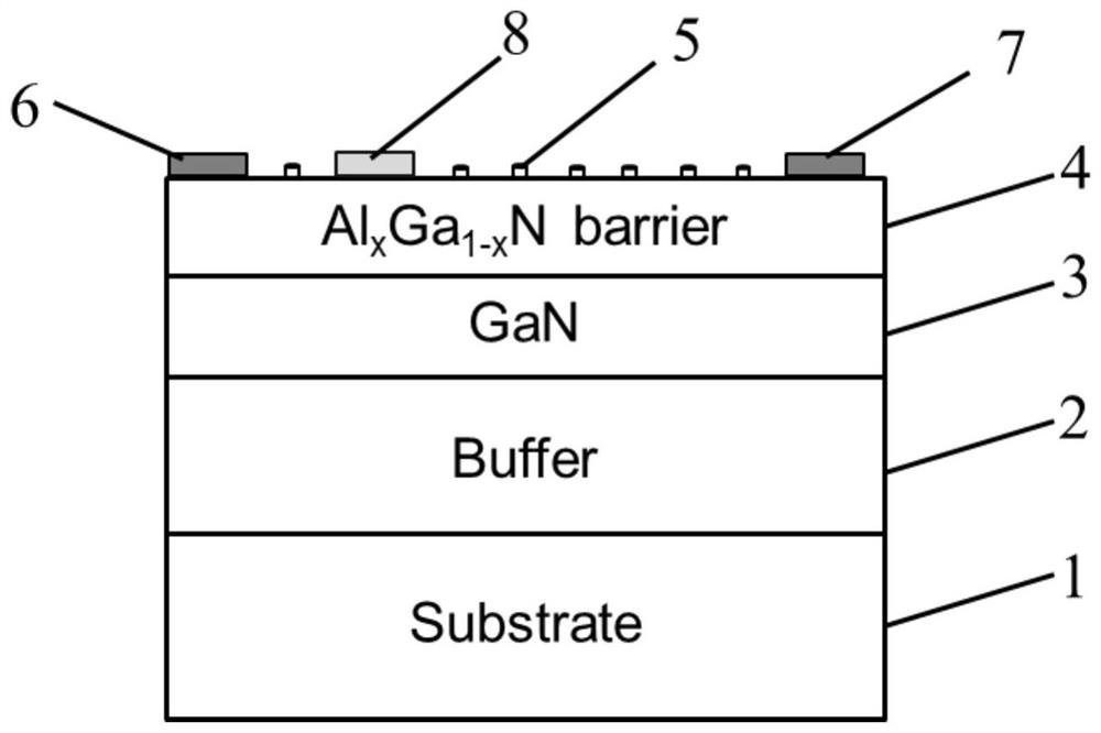
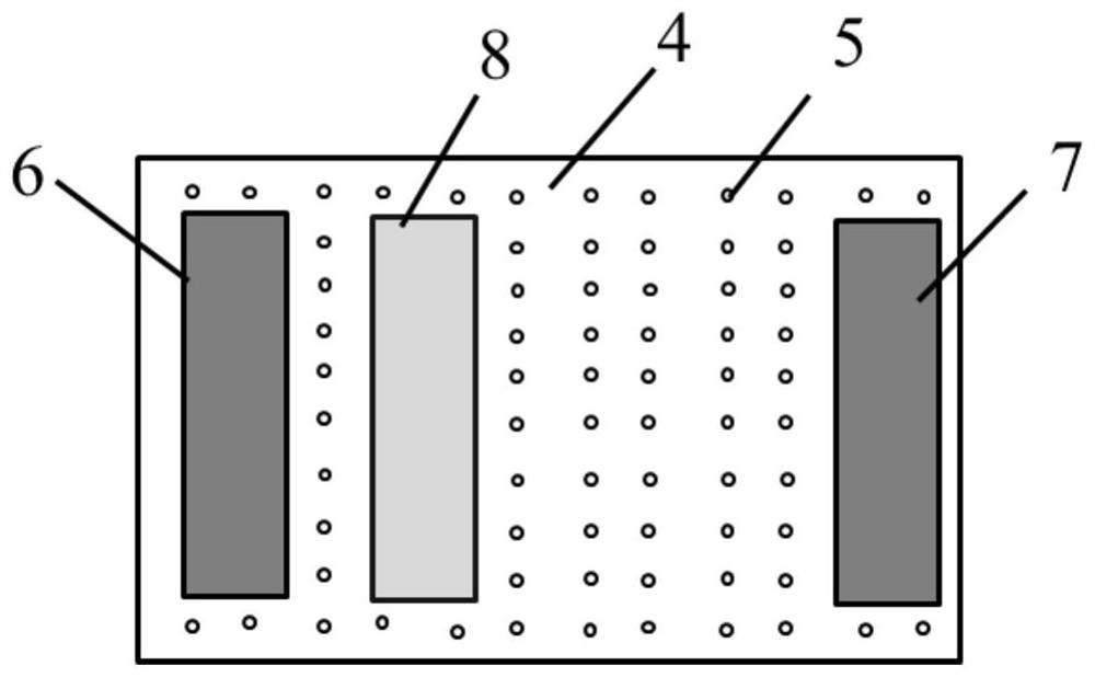
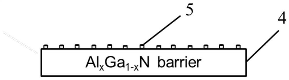
[0033] refer to figure 1 and figure 2 , a GaN transistor covering a nanocolumn barrier, comprising a substrate 1, a buffer layer 2, a channel layer 3 and a barrier layer 4 covering a nanocolumn 5 from bottom to top...


PUM

PropertyMeasurementUnit
heightaaaaaaaaaa

Abstract

Disclosed are a GaN transistor having a barrier covered by nanopillars and a preparation method therefor. AlxGa1-xN alloy nanopillars are distributed on the surface of a barrier layer of the transistor, and the nanopillars have one-to-one correspondence to screw dislocations in the barrier layer. According to the present invention, by controlling the TMGa flow rate and the V / III ratio in the growth process of an AlxGa1-xN barrier, the formation of V-shaped defects at termination positions of the screw dislocations can be avoided, and 1-3 nm AlxGa1-xN alloy nanopillars can be formed at the termination positions of the screw dislocations. As the V-shaped defects at the termination positions of the screw dislocations on the barrier surface are filled by the alloy nanopillars, the effective barrier thickness at the termination positions of the screw dislocations is increased, so that the gate leakage current is effectively suppressed and the withstand voltage characteristic of the transistor is improved.

Description

technical field [0001] The invention relates to the growth of semiconductor materials and the manufacture of semiconductor devices, in particular to a GaN-based transistor covered with nanocolumns and a barrier growth method thereof. Background technique [0002] GaN-based high electron mobility transistors (HEMTs) are made of Al x Ga 1-x N and GaN form a heterojunction, Al x Ga 1-x The interface spontaneous polarization and piezoelectric polarization discontinuity of the N / GaN heterojunction form remnant polarization charges, thereby forming a high-concentration two-dimensional electron gas at the interface. High quality Al x Ga 1-x The growth technology of the N barrier layer is one of the key epitaxial technologies for GaN-based transistors. GaN-based HEMTs have the advantages of high two-dimensional electron gas (2DEG) concentration, high mobility, and strong breakdown electric field, and are widely used in high-frequency and high-voltage microwave devices. [000...

Claims


Application Information

Patent Timeline
Patent Type & Authority Patents(China)
IPC IPC(8): H01L29/06H01L29/778H01L21/335B82Y30/00B82Y40/00
CPCB82Y30/00B82Y40/00H01L29/0665H01L29/66462H01L29/7787
Inventor 房育涛叶念慈
Owner HUNAN SANAN SEMICON CO LTD
Why Eureka
Try Eureka