Semiconductor device, fabrication method thereof and electronic device
A manufacturing method and semiconductor technology, applied in the direction of semiconductor devices, semiconductor/solid-state device manufacturing, electric solid-state devices, etc., can solve the problems of weak points in contact holes and easy formation of oxides, and reduce leakage current and reduce leakage current. Effect
- Summary
- Abstract
- Description
- Claims
- Application Information
AI Technical Summary
Problems solved by technology
Method used
Image

Examples
Embodiment 1
[0046] The following will refer to Figure 5A ~ Figure 5C A method for fabricating a semiconductor device according to an embodiment of the present invention will be described in detail. In this embodiment, the fabrication method of the semiconductor device of the present invention is described by taking the fabrication of the trench in the interlayer dielectric layer as an example.
[0047] First, if Figure 5A As shown, a semiconductor substrate 500 is provided, a device layer 501 is formed on the semiconductor substrate 500 , a trench 502 is formed in the device layer 501 , and a spacer 503 is formed on the surface of the trench 502 .
[0048] Wherein, the semiconductor substrate 500 can be at least one of the materials mentioned below: Si, Ge, SiGe, SiC, SiGeC, InAs, GaAs, InP or other III / V compound semiconductors, and also includes multiple semiconductors composed of these semiconductors. The layer structure or the like may be silicon-on-insulator (SOI), silicon-on-ins...
Embodiment 2
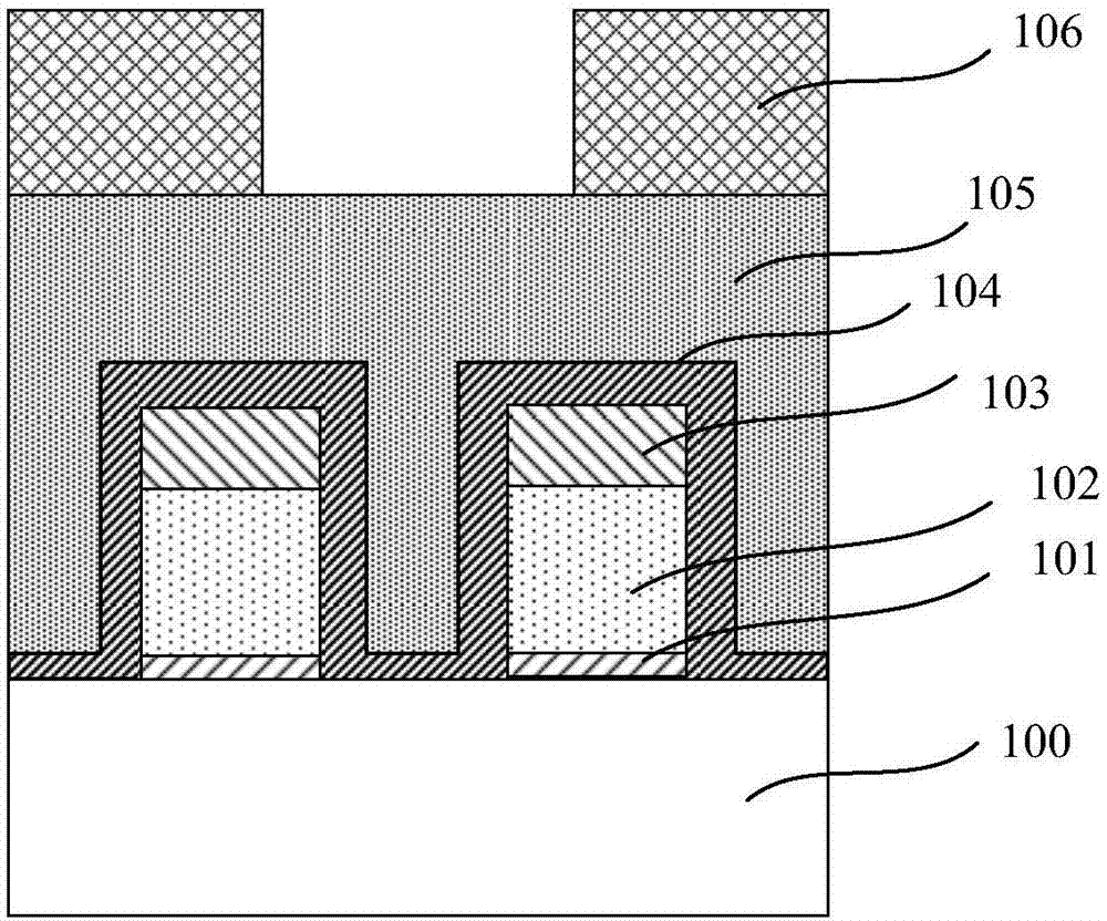
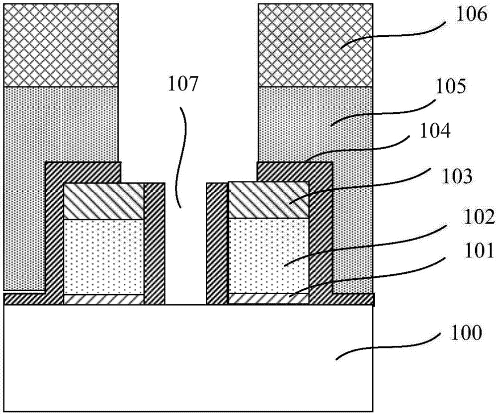
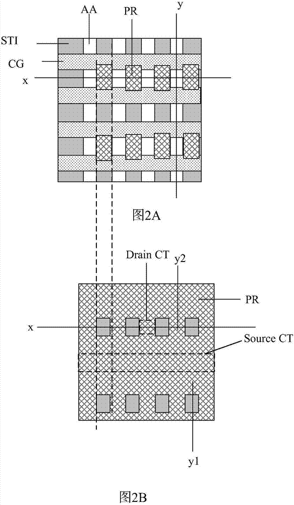
[0057] The following will refer to Figure 6A ~ Figure 6I A method for fabricating a semiconductor device according to an embodiment of the present invention will be described in detail. In this embodiment, the manufacturing method of the semiconductor device of the present invention is described by taking the manufacturing of the contact hole of the NOR device as an example. For the layout of the NOR device see Figure 2A shown in Figure 6A to Figure 6I For simplicity, only the device bit line orientation is shown (i.e., Figure 2A and Figure 2B Partial cross-sectional view in x-direction).
[0058] First, if Figure 6A As shown, a semiconductor substrate 600 is provided, and the semiconductor substrate 600 includes at least a storage area, and an isolation structure 601 and an active area AA separated by the isolation structure 601 are formed in the semiconductor substrate 600 of the storage area. A liner layer 602 and an interlayer dielectric layer 603 surrounding t...
Embodiment 3
[0089] The present invention also provides a semiconductor device fabricated by the above method, such as Figure 6I As shown, the semiconductor device includes: a semiconductor substrate 600, the semiconductor substrate 600 includes at least a storage area, and an isolation structure 601 and an active area AA separated by the isolation structure are formed in the semiconductor lining of the storage area. , a gate stack and an interlayer dielectric layer 603 surrounding the gate stack are formed on the semiconductor substrate 600 of the storage region, and a source contact and a drain are formed in the interlayer dielectric layer. A pole contact 607, wherein the drain contact has a vertical profile.
[0090] The drain contact of the semiconductor device in this embodiment has a vertical section, and the leakage current is reduced.
PUM
 Abstract
Description
Claims
Application Information
 - R&D
- Intellectual Property
- Life Sciences
- Materials
- Tech Scout
- Unparalleled Data Quality
- Higher Quality Content
- 60% Fewer Hallucinations
Browse by: Latest US Patents, China's latest patents, Technical Efficacy Thesaurus, Application Domain, Technology Topic, Popular Technical Reports.
© 2025 PatSnap. All rights reserved.Legal|Privacy policy|Modern Slavery Act Transparency Statement|Sitemap|About US| Contact US: help@patsnap.com