Circuit for reading and writing sram and sram data access method

A technology for reading and writing data and circuits, which is applied in the field of reading and writing SRAM circuits and SRAM data access. It can solve the problems of controlling the impact of clock quality, clock skew, timing problems, etc. The effect of skew or glitch

Active Publication Date: 2020-04-28
XIAN INTELLIGENCE SILICON TECH INC
View PDF7 Cites 0 Cited by
  • Summary
  • Abstract
  • Description
  • Claims
  • Application Information

AI Technical Summary

Problems solved by technology

This patent document has the following deficiencies: first, the read and write pulses and clocks in the prior art need to perform logical operations, which will have a certain impact on the quality of the control clock, which may cause clock skew or glitches, resulting in speed bottlenecks; second, The prior art read operation uses a parallel bus, which requires more internal wiring resources for distributed SRAM, and the parallel data interface spans a longer physical distance, resulting in a large delay and may cause timing problems; third, multiple clocks need to be used For input and read / write pulse input, more port resources need to be used, and the problem of signal crossing clock domains needs to be considered

Method used


Image

  • Circuit for reading and writing sram and sram data access method
  • Circuit for reading and writing sram and sram data access method
  • Circuit for reading and writing sram and sram data access method

Examples


Embodiment 1

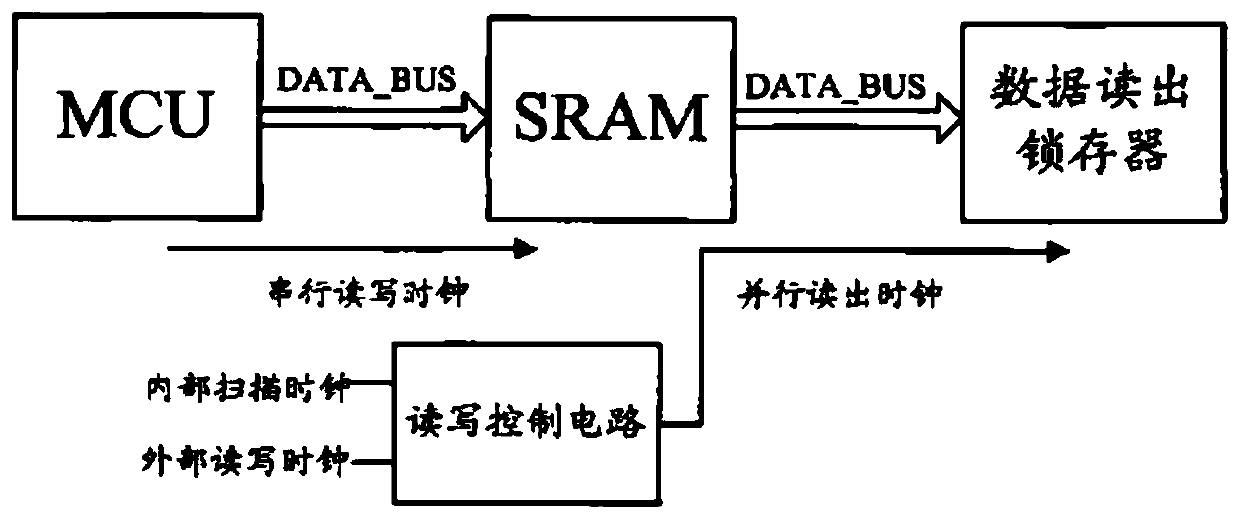
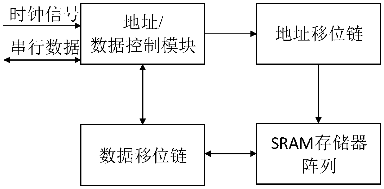
[0044] See figure 2 , image 3 and Figure 4 , figure 2 A schematic circuit diagram of a read-write SRAM provided by an embodiment of the present invention, image 3 A schematic diagram of a circuit structure of a read-write SRAM provided by an embodiment of the present invention, Figure 4 It is a flowchart of a method for reading and writing an SRAM provided by an embodiment of the present invention. .

[0045] The circuit includes: an address / data control module (Ad / Data control), an address shift chain (AddressShift Chain, abbreviated as ASC), a data shift chain (Data Shift Chain, abbreviated as DSC) and an SRAM memory array, wherein,

[0046] The address / data control module receives a clock signal (Clock, abbreviated as Clk) and serial data (Serial_data), and is used to decode the serial data in the clock signal and output a shift enable signal;

[0047] The address shift chain is connected to the address / data control module, and is used to receive the shift enabl...

Embodiment 2

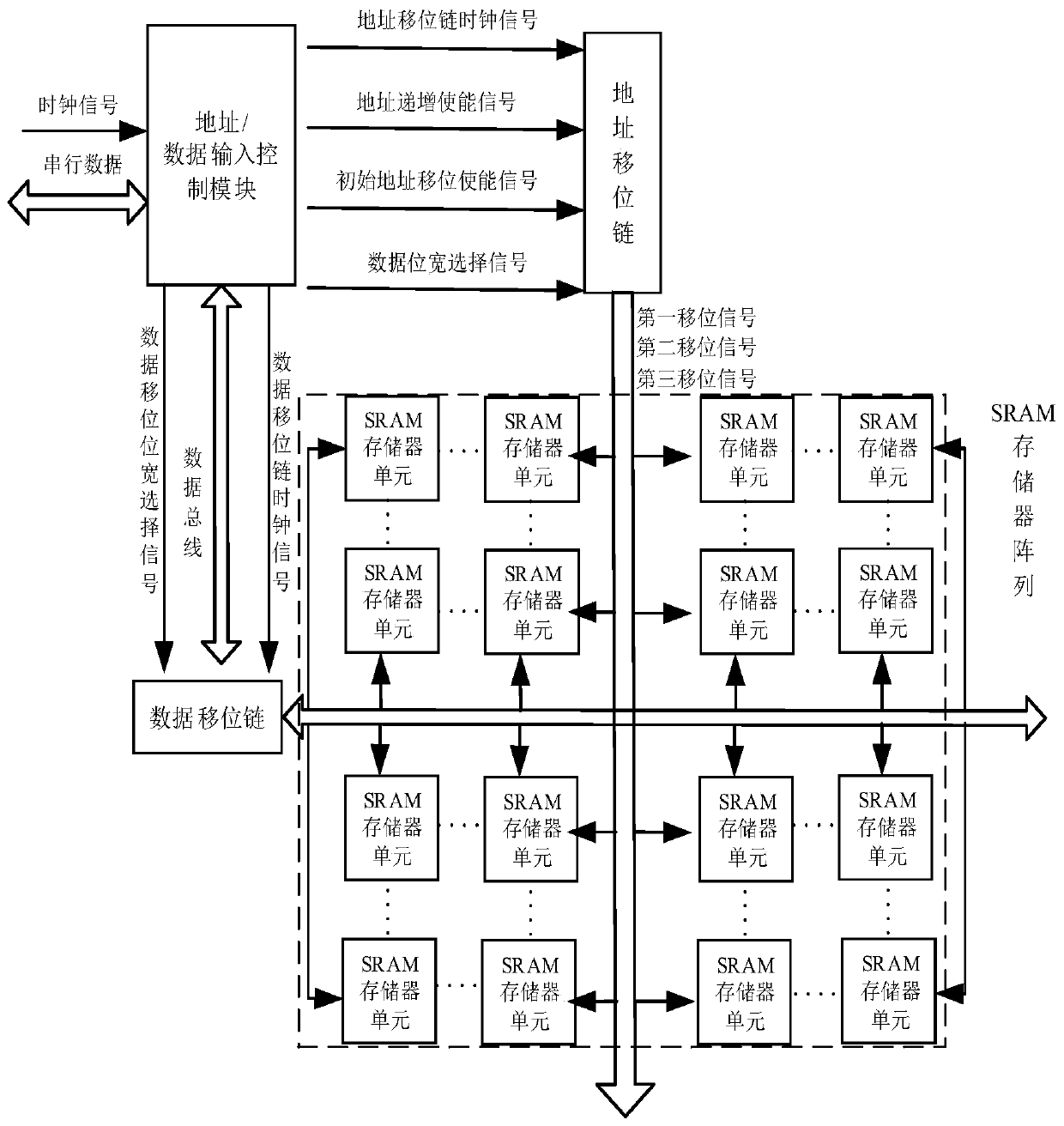
[0074] see again image 3 , this embodiment specifically describes the circuit for reading and writing SRAM of the present invention on the basis of the foregoing embodiments.

[0075] The address / data control module receives serial clock signals and serial data, wherein the initial address, data and instructions are all input to the address / data control module through the serial data interface;

[0076] The address / data control module transmits the clock signal of the address shift chain, the address increment enable signal and the initial address shift enable signal to the address shift chain, and the address / data control module controls the address shift chain to perform address shift operations. The shift chain transmits the address shift signal to the SRAM unit through the address shift bus, and performs an address shift increment operation through the address shift bus, and the address shift signal is determined by the data shift bit width selection signal.

[0077] Pre...

Embodiment 3

[0082] see again Figure 4 . This embodiment describes the method for reading and writing an SRAM of the present invention on the basis of the above embodiments. The specific method includes the following steps:

[0083] It mainly includes the following steps;

[0084] Step 1. Data loading;

[0085] Step 1.1, start the circuit and prepare for data reception;

[0086] Step 1.2, the address / data control module samples the received data according to the set data stream format and loads the initial address;

[0087] Step 1.3, the address / data control module loads the control instruction after the initial address is loaded.

[0088] Preferably, the control instructions include a single-row read instruction, a single-row write instruction, a read increment instruction, and a write increment instruction.

[0089] Step 2, the address / data control module judges whether to perform address increment;

[0090] Step 2.1, the address / data control module judges as no, then performs a ...


PUM


Abstract

The invention relates to an SRAM reading-writing circuit and an SRAM data accessing method. The circuit comprises an address / data control module, an address displacement chain, a data displacement chain and an SRAM memorizer array. The address / data control module receives clock signals and serial data and is used for coding the serial data in the clock signals and outputting a displacement instruction. The address displacement chain is connected to the address / data control module and used for receiving the displacement instruction of the address / data control module to conduct an address displacement operation. The data displacement chain is connected to the address / data control module and used for receiving a displacement enabling signal of the address / data control module to conduct a datadisplacement operation or used for transmitting the serial data of SRAM memorizers. The SRAM memorizer array is connected to the address displacement chain and the data displacement chain. The generation of a reading-writing control signal is completed through instruction coding, a same-clock-domain multi-stage register streamline mode is adopted in the circuit, and the circuit work efficiency isimproved.

Description

technical field [0001] The invention relates to the technical field of integrated circuits, in particular to a circuit for reading and writing SRAM and an SRAM data access method. Background technique [0002] FPGA (Field-Programmable Gate Array, Field Programmable Gate Array) is in PAL (Programmable Array Logic, programmable array logic), GAL (Generic Array Logic, general array logic), CPLD (Complex Programmable Logic Device, complex programmable logic device) and other programmable devices based on the further development of the product. It emerged as a semi-custom circuit in the field of ASIC (Application Specific Integrated Circuit), which not only solves the shortcomings of custom circuits, but also overcomes the shortcomings of the limited number of original programmable device gates. [0003] SRAM (Static Random Access Memory) has the advantages of high speed, low power consumption and compatibility with standard processes, and is widely used in PCs, personal communi...

Claims


Application Information

Patent Timeline
Patent Type & Authority Patents(China)
IPC IPC(8): G11C11/419G11C11/418
CPCG11C11/418G11C11/419
Inventor 王黎明古生霖贾红韦嶔程显志陈维新
Owner XIAN INTELLIGENCE SILICON TECH INC
Why Eureka
Try Eureka