
Planar transformer and manufacturing method

A technology of a planar transformer and a manufacturing method, applied in the field of transformers, can solve problems such as poor performance of planar transformers, and achieve the effects of flexible design method, high frequency and small leakage inductance

Active Publication Date: 2018-05-18
CHINA ZHENHUA GRP XINYUN ELECTRONICS COMP ANDDEV CO LTD
View PDF4 Cites 0 Cited by
  • Summary
  • Abstract
  • Description
  • Claims
  • Application Information

AI Technical Summary

Problems solved by technology

[0004] In view of this, an embodiment of the present invention provides a planar transformer and a manufacturing method to solve the problem of poor performance of planar transformers produced in the prior art

Method used


Image

  • Planar transformer and manufacturing method
  • Planar transformer and manufacturing method
  • Planar transformer and manufacturing method

Examples


no. 1 example

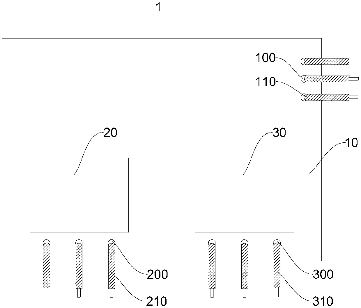
[0035] figure 1 A schematic diagram of the external structure of the planar transformer 1 provided by the embodiment of the present invention is shown. refer to figure 1 , The planar transformer 1 provided by the embodiment of the present invention includes: a PCB board 10 , a first magnetic core 20 , a second magnetic core 30 , an input lead 110 , a first output lead 210 and a second output lead 310 . Wherein, the first magnetic core 20 and the second magnetic core 30 are embedded on the PCB board 10, and the input lead-out hole 100, the first output lead-out hole 200 and the second output lead-out hole 300 are opened through the PCB board 10, and the input lead 110 is soldered On the input lead-out hole 100 , the first output lead 210 is welded on the first output lead-out hole 200 , and the second output lead 310 is welded on the second output lead-out hole 300 .

[0036] The planar transformer 1 can actually be regarded as composed of a first sub-transformer and a second...

no. 2 example

[0047] Figure 6 A flow chart of a method for manufacturing a planar transformer provided by an embodiment of the present invention is shown. See Figure 6 , the method includes:

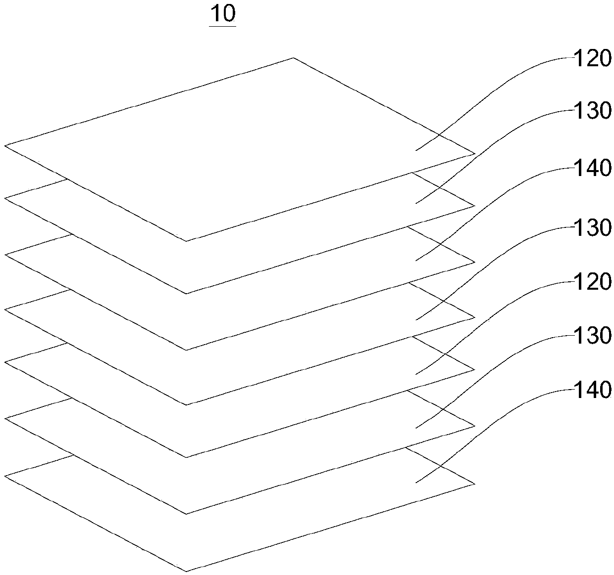
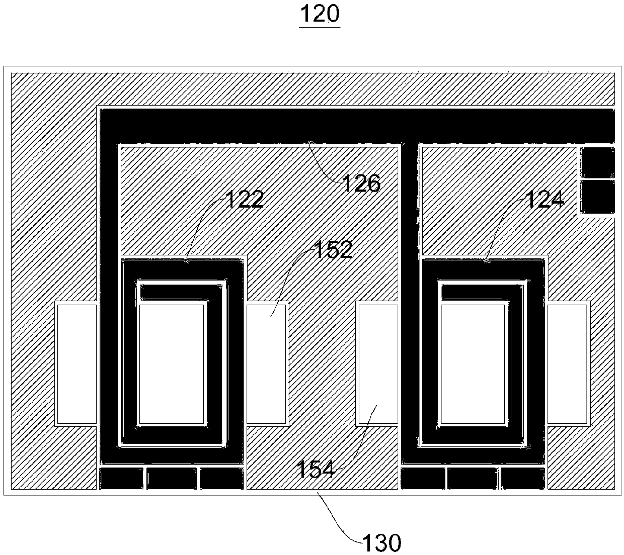
[0048] Step S1: Etching on the primary copper layer 120 produces a first primary winding 122, a second primary winding 124 and a common copper wire 126, the first primary winding 122 and the second primary winding 124 are connected to the common copper wire 126 electrical connections.

[0049] Step S2 : Etching the secondary copper layer 140 to produce the first secondary winding 142 and the second secondary winding 144 .

[0050] In steps S1 and S2, the windings of the first sub-transformer and the second sub-transformer are produced by etching on the copper layer. Compared with the method of winding the copper wire on the magnetic core of the wire-wound transformer, the uncertainty factor is small and consistent. Good performance, convenient for rapid mass production.

[0051] Step S3: stack ...


PUM

PropertyMeasurementUnit
thicknessaaaaaaaaaa

Abstract

The invention relates to the technical field of transformers, and provides a planar transformer and manufacturing method. The planar transformer comprises a PCB, a first magnetic core and a second magnetic core, wherein the PCB comprises primary copper layers, insulating medium layers and secondary copper layers; the primary copper layers and the secondary copper layers are sequentially and alternately laminated; each of the insulating medium layers is arranged between each of the primary copper layers and each of the secondary copper layers adjacent to each other; each of the primary copper layers comprises a first primary winding, a second primary winding and a common copper wire; each of the first primary winding and each of the second primary winding are both electrically connected with each of the common copper wire; each of the secondary copper layer comprises a first secondary winding and a second secondary winding; first magnetic cores are mounted in first through holes formedin each of the first primary winding and each of the first secondary winding; second cores are mounted in second through holes formed in each of the second primary winding and each of the second secondary winding. The planar transformer has the advantages of small size, good consistency, quick heat dissipation, low loss consumption, high frequency, small leakage inductance, stability, reliability,strong function, wide application range and the like.

Description

technical field [0001] The invention relates to the technical field of transformers, in particular to a planar transformer and a manufacturing method. Background technique [0002] With the development of electronic circuits towards high frequency, high power transmission efficiency, high power density, high reliability, high stability, and high integration, higher requirements are put forward for the design of transformers in power circuits. The leakage inductance and distributed capacitance of traditional wire-wound transformers make it difficult to control their batch consistency, which brings great difficulty to the batch production and debugging of power circuits. At the same time, the three-dimensional structure of traditional wire-wound transformers takes up a large The volume is no longer suitable for the current development trend of flattening power circuits. At the same time, due to the limitations of its design ideas and application environment, it cannot meet th...

Claims


Application Information

Patent Timeline
Patent Type & Authority Applications(China)
IPC IPC(8): H01F27/28H01F27/26H01F41/04H01F41/10
Inventor 李国强况光禄吴明春邓伟袁文杰代东升
Owner CHINA ZHENHUA GRP XINYUN ELECTRONICS COMP ANDDEV CO LTD
Learn More