Supercharge Your Innovation With Domain-Expert AI Agents!

Electronic device packaging tape

A technology of electronic devices and adhesive tapes, applied in the direction of electric solid devices, electrical components, semiconductor devices, etc., can solve problems such as warping of electronic device packages, and achieve the effect of suppressing voids

Active Publication Date: 2021-01-15
FURUKAWA ELECTRIC CO LTD
View PDF8 Cites 0 Cited by
  • Summary
  • Abstract
  • Description
  • Claims
  • Application Information

AI Technical Summary

Problems solved by technology

Electronic device packages warp due to this difference

Method used


Image

  • Electronic device packaging tape
  • Electronic device packaging tape
  • Electronic device packaging tape

Examples


preparation example Construction

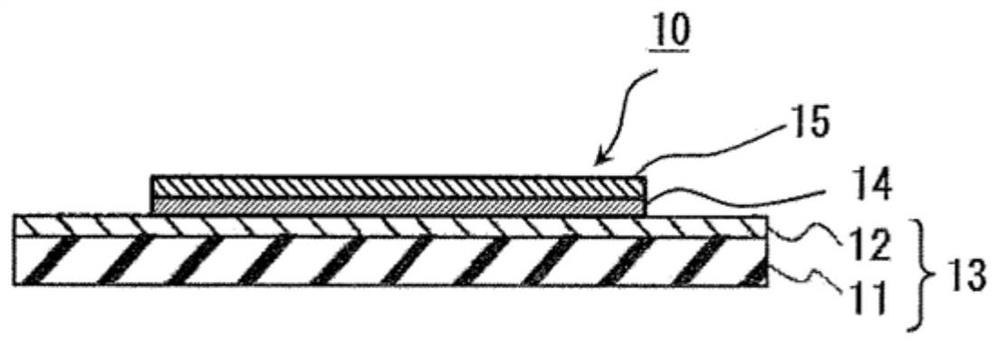
[0040]The preparation of the acrylic polymer can be carried out by applying an appropriate method such as a solution polymerization method, an emulsion polymerization method, a bulk polymerization method, and a suspension polymerization method to a mixture of one or more component monomers. From the viewpoint of preventing wafer contamination, the adhesive layer 12 preferably suppresses the composition containing low molecular weight substances. From this viewpoint, it is preferable to use an acrylic polymer having a weight average molecular weight of 300,000 or more, especially 400,000 to 3 million. As the main component, the adhesive can also be an appropriate crosslinking type based on an internal crosslinking method or an external crosslinking method.

[0041]In addition, in order to control the cross-linking density of the adhesive layer 12 and improve the pick-up properties, for example, the use of polyfunctional isocyanate-based compounds, polyfunctional epoxy-based compounds, m...

Embodiment 2~4、 comparative example 1~4

[0182]The electronic devices of Examples 2 to 4 and Comparative Examples 1 to 4 were produced by the same method as Example 1, except that the combination of the adhesive tape, adhesive layer composition, and metal layer was set to the combination described in Table 1. Tape for packaging.

[0183]The following measurements and evaluations were performed on the electronic device packaging tapes of Examples 1 to 4 and Comparative Examples 1 to 4. The results are shown in Table 1.

[0184](Storage modulus)

[0185]The storage elastic modulus at 25°C of the adhesive layer used in each example and each comparative example was measured as follows. Adhesion of the adhesive layer used in each example and comparative example on a polyethylene terephthalate (PET) separator with a thickness of 25μm so that the film thickness after drying will reach 30μm After the agent layer composition is dried, it is attached to a polyethylene terephthalate (PET) separator with a thickness of 25 μm, the adhesive laye...


PUM

PropertyMeasurementUnit
storage modulusaaaaaaaaaa
particle sizeaaaaaaaaaa
densityaaaaaaaaaa

Abstract

The present invention provides a tape for encapsulating electronic devices capable of suppressing warping of a laminated body of a semiconductor, an adhesive layer, and a semiconductor chip during pre-curing of an adhesive layer, and capable of suppressing sticking during flip-chip connection. Voids are created in the adhesive layer. The tape for encapsulating electronic devices according to the present invention is characterized by comprising: an adhesive tape having a base film and an adhesive layer; a metal layer laminated on the side opposite to the base film of the adhesive layer; And an adhesive layer disposed on the side opposite to the adhesive layer of the metal layer and used to bond the metal layer to the back of the electronic device, the adhesive layer is heated at 100°C for 3 hours at 25°C The storage elastic modulus is 10 GPa or less, and the curing rate when heated at 100° C. for 3 hours is 10 to 100%.

Description

Technical field[0001]The present invention relates to a tape for packaging electronic devices, in particular to a tape for packaging electronic devices with a metal layer.Background technique[0002]In recent years, electronic devices such as mobile phones and notebook PCs have been required to be further thinner and smaller. For this reason, in order to reduce the thickness and size of electronic device packages such as semiconductor packages mounted on electronic devices, the number of electrodes of electronic devices and circuit boards has been increased, and the pitch has also been narrowed. Such electronic device packages include, for example, Flip Chip (FC; Flip Chip) mounting packages.[0003]In the flip-chip mounting package, since the number of electrodes is increased or the pitch is narrowed as described above, an increase in heat generation becomes a problem. For this reason, as a heat dissipation structure of a flip-chip package, it is proposed to provide a metal layer via a...

Claims


Application Information

Patent Timeline
Patent Type & Authority Patents(China)
IPC IPC(8): H01L23/29H01L23/40H01L21/683B32B15/092B32B15/08B32B7/12C09J7/30C09J11/04C09J11/08C09J133/00C09J163/00C09J201/00C09J7/20
CPCC09J11/04C09J11/08C09J133/00C09J163/00C09J201/00H01L23/00C09J7/20
Inventor 佐野透杉山二朗青山真沙美石黑邦彦
Owner FURUKAWA ELECTRIC CO LTD
Features
  • R&D
  • Intellectual Property
  • Life Sciences
  • Materials
  • Tech Scout
  • Unparalleled Data Quality
  • Higher Quality Content
  • 60% Fewer Hallucinations
Learn More