Preparation method of low-stress silicon carbide single crystal and apparatus of same
A silicon carbide single crystal, low-stress technology, applied in chemical instruments and methods, single crystal growth, single crystal growth, etc., can solve the problems of no effect, high energy consumption cost, long cycle, etc., to reduce production costs , short annealing time, and the effect of improving the surface quality
- Summary
- Abstract
- Description
- Claims
- Application Information
AI Technical Summary
Problems solved by technology
Method used
Image

Examples
Embodiment 1
[0027] A method for preparing a low-stress silicon carbide single crystal is realized by the following crystal growth device:
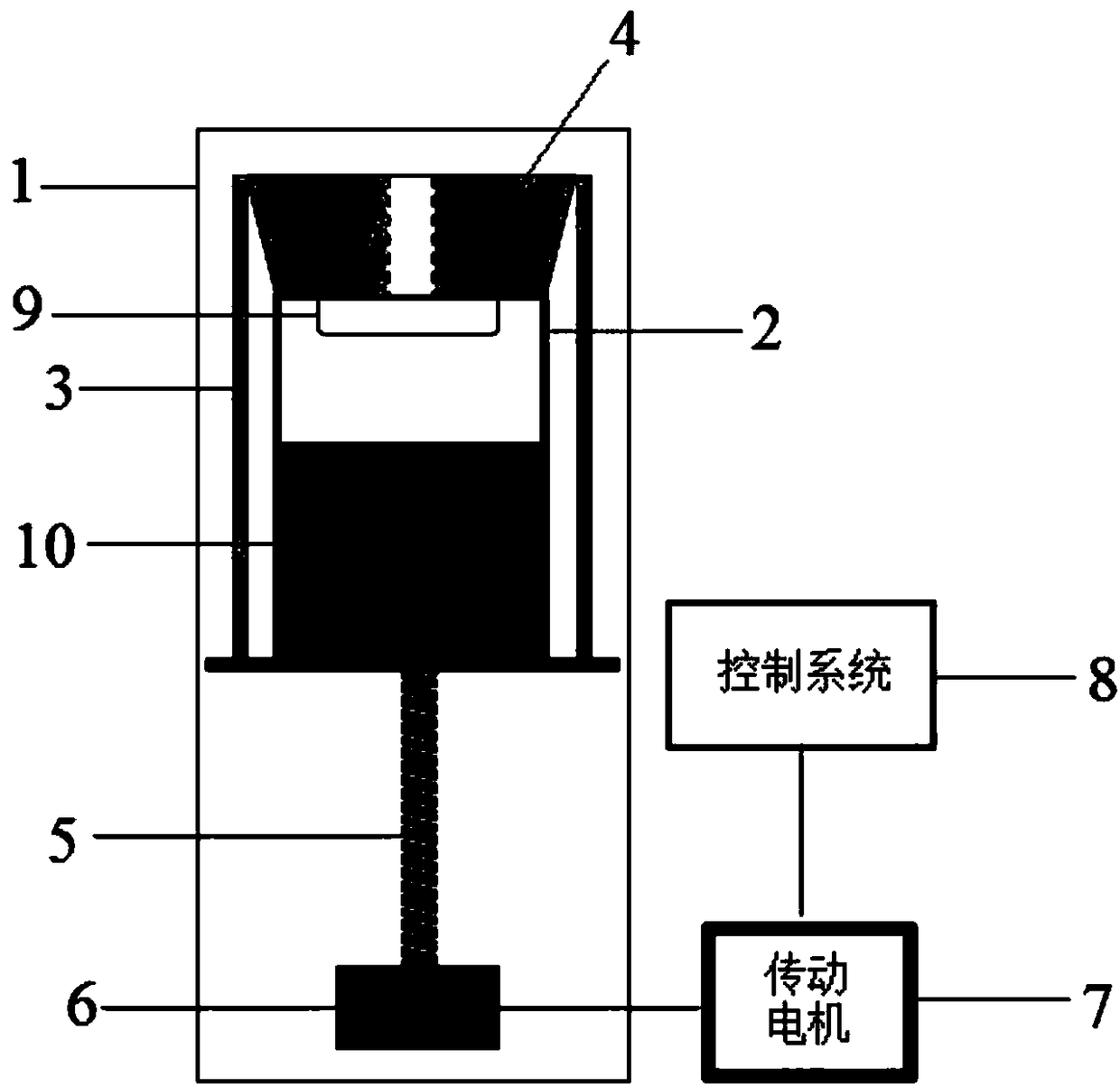
[0028] This crystal growth device comprises growth furnace 1, and growth furnace 1 is provided with graphite crucible 2, and the exterior of graphite crucible 2 is provided with side insulation layer I3, and the top of graphite crucible 2 is provided with upper insulation layer II4, and described upper insulation layer II4 is a wedge-shaped structure with an inclination angle, so that the thickness of the upper insulation layer II4 decreases linearly from the center to the edge; the lower part of the graphite crucible 2 is provided with a transmission rod 5 and a transmission device 6 in turn; the longitudinal axis of the graphite crucible 2, the longitudinal axis of the transmission rod 5 and the The longitudinal axis of growth furnace 1 is on the same straight line;
[0029] Concrete preparation steps are:
[0030] (1) Place the crystal growth devi...
Embodiment 2
[0042] A method for preparing a low-stress silicon carbide single crystal is realized by the following crystal growth device:
[0043] This crystal growth device comprises growth furnace 1, and growth furnace 1 is provided with graphite crucible 2, and the exterior of graphite crucible 2 is provided with side insulation layer I3, and the top of graphite crucible 2 is provided with upper insulation layer II4, and described upper insulation layer II4 is a wedge-shaped structure with an inclination angle, so that the thickness of the upper insulation layer II4 decreases linearly from the center to the edge; the lower part of the graphite crucible 2 is provided with a transmission rod 5 and a transmission device 6 in turn; the longitudinal axis of the graphite crucible 2, the longitudinal axis of the transmission rod 5 and the The longitudinal axis of growth furnace 1 is on the same straight line;
[0044] Concrete preparation steps are:
[0045] (1) Place the crystal growth devi...
Embodiment 3
[0057] A method for preparing a low-stress silicon carbide single crystal is realized by the following crystal growth device:
[0058] This crystal growth device comprises growth furnace 1, and growth furnace 1 is provided with graphite crucible 2, and the exterior of graphite crucible 2 is provided with side insulation layer I3, and the top of graphite crucible 2 is provided with upper insulation layer II4, and described upper insulation layer II4 is a wedge-shaped structure with an inclination angle, so that the thickness of the upper insulation layer II4 decreases linearly from the center to the edge; the lower part of the graphite crucible 2 is provided with a transmission rod 5 and a transmission device 6 in turn; the longitudinal axis of the graphite crucible 2, the longitudinal axis of the transmission rod 5 and the The longitudinal axis of growth furnace 1 is on the same straight line;
[0059] Concrete preparation steps are:
[0060] (1) Place the crystal growth devi...
PUM
| Property | Measurement | Unit |
|---|---|---|
| warpage | aaaaa | aaaaa |
| warpage | aaaaa | aaaaa |
| warpage | aaaaa | aaaaa |
Abstract
Description
Claims
Application Information
 - R&D
- Intellectual Property
- Life Sciences
- Materials
- Tech Scout
- Unparalleled Data Quality
- Higher Quality Content
- 60% Fewer Hallucinations
Browse by: Latest US Patents, China's latest patents, Technical Efficacy Thesaurus, Application Domain, Technology Topic, Popular Technical Reports.
© 2025 PatSnap. All rights reserved.Legal|Privacy policy|Modern Slavery Act Transparency Statement|Sitemap|About US| Contact US: help@patsnap.com