Seed crystal bonding method for growing SiC crystals

A seed crystal and crystal technology, applied in the field of crystal growth, to achieve the effects of uniform growth, quality improvement, and uniform thickness distribution

Inactive Publication Date: 2012-07-04
SHANGHAI INST OF CERAMIC CHEM & TECH CHINESE ACAD OF SCI
View PDF4 Cites 8 Cited by
  • Summary
  • Abstract
  • Description
  • Claims
  • Application Information

AI Technical Summary

Problems solved by technology

[0005] In order to solve the problem of bonding and fixing seed crystals in SiC crystals grown by physical vapor transport (PVT), the present invention discloses a seed crystal bonding method for growing high-quality SiC crystals, which can uniformly bond and fix SiC seed crystals ...

Method used


Image

  • Seed crystal bonding method for growing SiC crystals
  • Seed crystal bonding method for growing SiC crystals
  • Seed crystal bonding method for growing SiC crystals

Examples


Embodiment 1

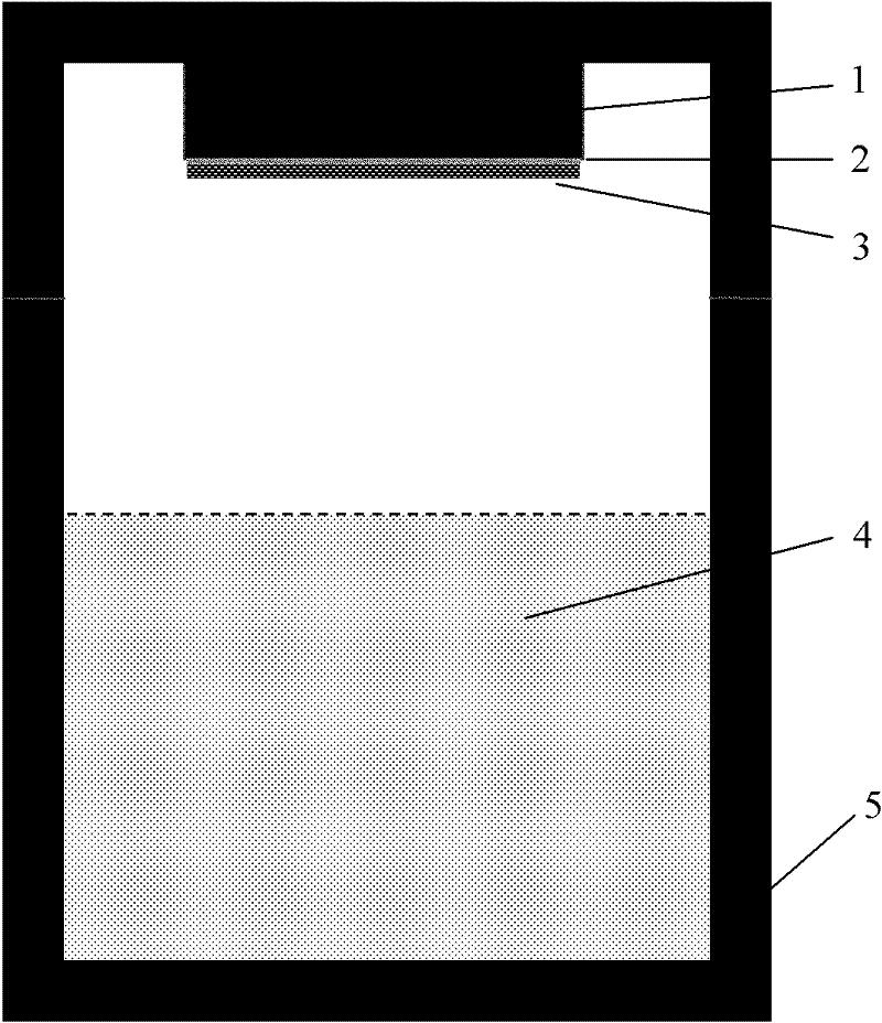
[0035] A seed crystal bonding method for growing high-quality SiC crystals, comprising the steps of:

[0036] 1. Carry out the necessary leveling, processing and cleaning of the seed crystal holder, and use a heating platform to heat the seed crystal holder, seed crystal and edible white sugar to 120°C, so that the white sugar can be melted into fluid liquid white sugar, which is easy to paint evenly.

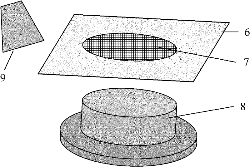
[0037] 2. The silk screen 7 (the wire diameter of the screen is 0.05mm) that adopts 80 mesh polyester material is covered on the seed crystal holder 8 (such as figure 2 As shown), after smearing liquid white sugar on the screen 7, use the brush 9 to brush and scrape the liquid white sugar to ensure that the liquid white sugar is evenly distributed in the brushing area, and finally separate the screen from the seed crystal holder.

[0038] 3. Place the seed crystal on the seed crystal support coated with liquid white sugar, and then use a self-made metal structure pressure devi...

Embodiment 2

[0041] A seed crystal bonding method for growing high-quality SiC crystals, comprising the steps of:

[0042] 1. Carry out the necessary leveling, processing and cleaning of the seed crystal holder, and use a heating platform to heat the seed crystal holder, seed crystal and AB glue to 40°C, so that the AB glue is in a fluid state, which is convenient for even coating.

[0043] 2. The wire mesh 7 (the wire diameter of the wire mesh is 0.02mm) that adopts 120 mesh stainless steel wire materials is covered on the seed crystal holder 8 (such as figure 2 As shown), after smearing the flowable AB glue on the screen 7, use the brush 9 to brush and scrape the flowy AB glue to ensure that the flowy AB glue is evenly distributed in the brushing area, and finally the screen and the seed crystal Support separation.

[0044] 3. Bond the seed crystal on the seed crystal support coated with flowable AB glue, and then use a self-made metal structure pressure device (a metal fixture) to app...

Embodiment 3

[0047] A seed crystal bonding method for growing high-quality SiC crystals, comprising the steps of:

[0048] 1. Use 502 glue as the adhesive at room temperature (about 20-30°C).

[0049] 2. Carry out necessary leveling, processing and cleaning of the seed crystal holder, and then cover the seed crystal holder 8 with a wire mesh 7 (the wire diameter of the wire mesh is 0.07 mm) made of 40 mesh stainless steel wire (such as figure 2 shown), after smearing the flowable 502 glue on the screen 7, use the brush 9 to brush and scrape the flowy 502 glue to ensure that the flowy 502 glue is evenly distributed in the brushing area, and then quickly put the screen and the seed Crystal holder separated.

[0050] 3. Quickly bond the seed crystal to the seed crystal holder coated with flowable 502 glue, and then use a self-made metal structure pressure device (a metal fixture) to apply appropriate pressure evenly on the seed crystal and the seed crystal holder to make the seed crystal T...


PUM

PropertyMeasurementUnit
Thicknessaaaaaaaaaa
Thicknessaaaaaaaaaa
Wire diameteraaaaaaaaaa

Abstract

The invention belongs to the field of crystal growth, and relates to a seed crystal bonding method for growing SiC crystals. The seed crystal bonding method for growing high-quality SiC crystal comprises the following steps of: (1) printing a silk screen; (2) bonding the seed crystals; and (3) curing an adhesive for bonding the seed crystals and a seed crystal support, wherein the thickness of the cured adhesive layer is 7-10 microns. The seed crystal bonding method for growing the high-quality SiC crystals provided by the invention can ensure uniform distribution of the thickness of the adhesive layer between the seed crystals and the seed crystal support and avoid cracking caused by non-uniform mechanical stress and heat stress; and meanwhile, the temperature gradient distribution of the seed crystals is uniform, thereby being beneficial to the uniform growth of the SiC crystals, and further improving the quality of the SiC crystals.

Description

technical field [0001] The invention belongs to the field of crystal growth and relates to a seed crystal bonding method for growing high-quality SiC crystals. Background technique [0002] Modern industrial technologies such as microelectronics, optoelectronics and information technology have achieved rapid development on the basis of the first generation of semiconductor materials represented by silicon and the second generation of semiconductor materials represented by gallium arsenide, and are widely used in aerospace, nuclear energy, communication , national defense security and other fields. At the same time, the development of modern industrial technology has put forward higher requirements for semiconductor materials and devices. Semiconductor materials such as silicon and gallium arsenide are limited by their own structure and performance, and cannot meet the requirements of applications such as high temperature, high frequency, and high power. In contrast, silico...

Claims


Application Information

Patent Timeline
IPC IPC(8): C30B23/00C30B29/36
Inventor 孔海宽严成锋忻隽陈建军肖兵陈之战杨建华施尔畏
Owner SHANGHAI INST OF CERAMIC CHEM & TECH CHINESE ACAD OF SCI
Why Eureka
Try Eureka