Optical communication waveband polymer waveguide grating coupler and manufacturing method thereof

A technology of waveguide grating and manufacturing method, which is applied in the direction of optical waveguide light guide, light guide, optics, etc., can solve the problems of restricting the application of functional chips, achieve the effect of reducing the manufacturing cost, avoiding the manufacturing process, and reducing the resolution of photolithography

Pending Publication Date: 2018-06-01
FUZHOU UNIV
View PDF0 Cites 9 Cited by
  • Summary
  • Abstract
  • Description
  • Claims
  • Application Information

AI Technical Summary

Problems solved by technology

Such shortcomings greatly limit the application of polymer-based integrated photoni

Method used


Image

  • Optical communication waveband polymer waveguide grating coupler and manufacturing method thereof
  • Optical communication waveband polymer waveguide grating coupler and manufacturing method thereof
  • Optical communication waveband polymer waveguide grating coupler and manufacturing method thereof

Examples


Embodiment Construction

[0047] The present invention will be further described in detail below in conjunction with the accompanying drawings and specific embodiments.

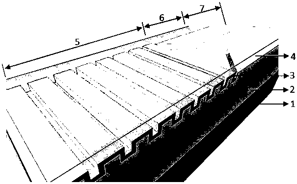
[0048] The invention provides a polymer waveguide grating coupler in the optical communication band, such as figure 1 As shown, it includes a waveguide coupling grating structure and a waveguide structure. The waveguide coupling grating structure is composed of a substrate 1, a low refractive index waveguide lower cladding layer 2, a high refractive index dielectric layer 3, a high refractive index waveguide core layer 4 and an air layer. , the waveguide structure is composed of a substrate 1, a low-refractive index waveguide lower cladding layer 2, a high-refractive index waveguide core layer 4 and an air layer. The waveguide coupling grating structure and the waveguide structure are integrally fabricated on the same substrate, and the two are effectively connected through a high refractive index waveguide core layer. According to s...


PUM

PropertyMeasurementUnit
Angle of incidenceaaaaaaaaaa

Abstract

The invention relates to an optical communication waveband polymer waveguide grating coupler and a manufacturing method thereof. The waveguide grating coupler comprises a grating structure and a waveguide structure, wherein the grating structure is composed of a substrate, a low-refractive-index waveguide lower coverage layer, a high-refractive-index medium layer, a high-refractive-index waveguidecore layer and an air layer; the waveguide structure is composed of a substrate, a low-refractive-index waveguide lower coverage layer, a high-refractive-index waveguide core layer and an air layer.A key preparation technology of the waveguide grating coupler comprises the following steps: manufacturing a main mold and a soft secondary mold; manufacturing the substrates and the low-refractive-index waveguide lower coverage layers of the grating structure and the waveguide structure; manufacturing the high-refractive-index medium layer of the grating structure; spinning and covering a high-refractive-index polymer waveguide core layer material. The optical communication waveband polymer waveguide grating coupler and the manufacturing method thereof have the advantages of simple realization technology and low cost; the difficulty of aligning a polymer waveguide and a common single-mode optical fiber through an end face coupling manner can be effectively reduced, and application researches of a polymer integrated photonic device in the aspects of optical sensing and optical interconnection are easily propelled.

Description

technical field [0001] The invention relates to the technical field of structural design and manufacturing of polymer integrated photonic devices, in particular to a polymer waveguide grating coupler in the optical communication band and a manufacturing method thereof. Background technique [0002] Photonic integration technology has shown great potential in the field of optical sensing and optical communication. Currently, the technology is being developed simultaneously on several different material platforms, such as silicon dioxide (SiO 2 ), silicon-on-insulator (SOI, Silicon-on-insulator), indium phosphide (InP, Indium phosphide) and organic polymers, etc. Compared with inorganic materials, organic polymer integrated photonic devices have obvious advantages in terms of adjustable refractive index, simple preparation process, and low cost. At the same time, the good flexibility of the material itself can be used "naturally" for flexible integrated photonic chips and op...

Claims


Application Information

Patent Timeline
IPC IPC(8): G02B6/124G02B6/13
CPCG02B6/124G02B6/13
Inventor 王凌华张雅珍王少昊
Owner FUZHOU UNIV
Why Eureka
Try Eureka