Preparation method of superconductive Josephson junction

A superconducting and substrate technology, which is used in the manufacture/processing of superconducting devices, devices containing a node of different materials, superconducting devices, etc. , difficult to control and other problems, to avoid the preparation process of the suspension glue, reduce the difficulty, and achieve the effect of high control accuracy

Active Publication Date: 2018-06-01
ORIGIN QUANTUM COMPUTING TECH (HEFEI) CO LTD
View PDF4 Cites 13 Cited by
  • Summary
  • Abstract
  • Description
  • Claims
  • Application Information

AI Technical Summary

Problems solved by technology

[0005] Aiming at the problem that the suspended glue structure in the prior art has high requirements on the properties of the glue and the control precision of the electron beam exposure dose, the control is difficult, and the suspended glue is very fragile and cannot withstand high-intensity cleaning, which greatly limits the follow-up process. The invention provides a preparation method of the superconducting Josephson junction of the main circuit element in the superconducting qubit

Method used


Image

  • Preparation method of superconductive Josephson junction
  • Preparation method of superconductive Josephson junction
  • Preparation method of superconductive Josephson junction

Examples


preparation example Construction

[0047]The preparation method of the superconducting Josephson junction of the present embodiment, its steps are:

[0048] 1) Substrate pretreatment

[0049] A material with a resistivity > 10000 ohm*cm is selected as the substrate; a silicon wafer with a high resistance value is preferred.

[0050] The substrate is cleaned, and the cleaning method may be ultrasonic cleaning. Then transfer the substrate to a container containing isopropanol (IPA) for immersion, then transfer the substrate to a container containing deionized water (DI) for immersion, and finally take out the substrate and dry it with inert gas. sheet, to obtain a clean substrate;

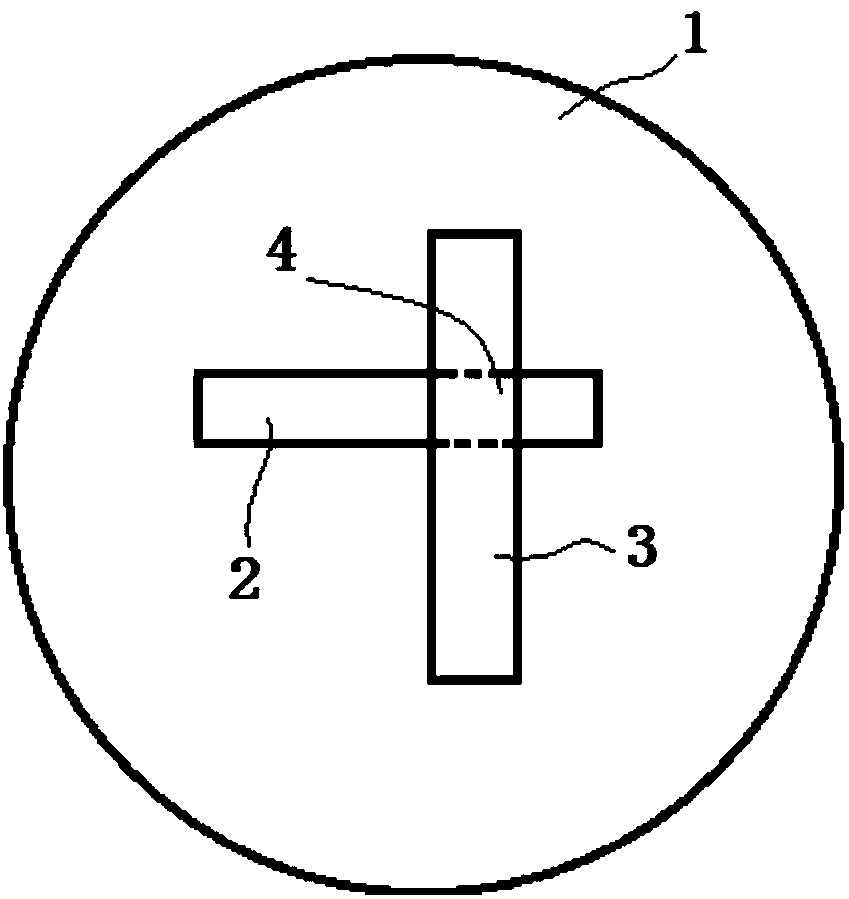
[0051] 2) Electron beam exposure

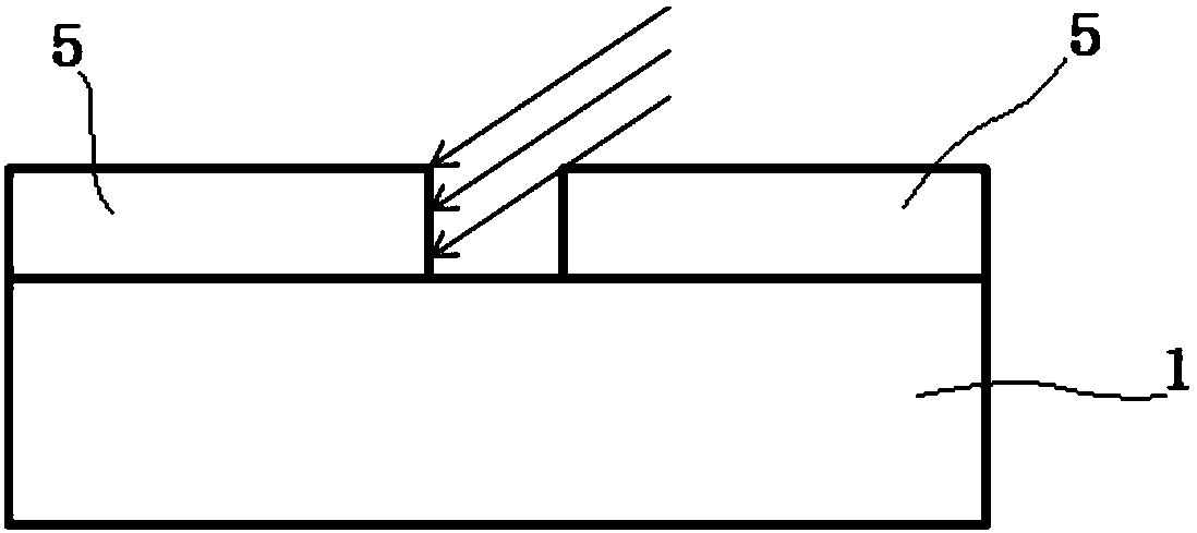
[0052] Coating electron beam glue 5 on the substrate, using electron beam exposure equipment to expose two regions A region and B region on the substrate, A region 2 and B region 3 have intersecting region C region 4; according to different electron beam glue, baking Select the appropriate exposu...

Embodiment 1

[0061] The method for preparing superconducting Josephson junction in this embodiment is as follows:

[0062] 1) Substrate pretreatment, clean the substrate:

[0063] Put a high-resistance silicon wafer (with a resistance value of 10050 ohm*cm) in a beaker filled with 1-methyl-2-pyrrolidone (NMP) solution and vibrate ultrasonically for 3 minutes, then transfer the substrate to a beaker filled with isopropanol (IPA ) solution in a beaker for 3 minutes, and finally put the substrate in deionized water (DI) solution and ultrasonically vibrate for 3 minutes. 100%, making the substrate clean enough for the next step. Here, the ultrasonic time can be controlled at more than 3 minutes to achieve the technical purpose, preferably 3 minutes to 5 minutes in order to improve the experimental efficiency.

[0064] 2) Electron beam exposure

[0065] Put a single layer of MMA glue on the cleaned silicon wafer and a layer of PMMA950A4 glue evenly, and the thickness of the electron beam glu...

Embodiment 2

[0076] The method for preparing superconducting Josephson junction in this embodiment is as follows:

[0077] 1) Substrate pretreatment: the substrate is made of a high-resistance silicon chip (10000 ohms*cm is used in this embodiment), and the high-resistance silicon chip is first placed in a beaker filled with 1-methyl-2-pyrrolidone (NMP) solution and ultrasonically Vibrate for 4min, then transfer the substrate to a beaker filled with isopropanol (IPA) solution and ultrasonically vibrate for 4min, finally put the substrate in deionized water (DI) solution Clamp the sample with tweezers and blow out the sample with a nitrogen chamber, and the ultrasonic power is 100%, so that the substrate can reach a clean level suitable for the next step;

[0078] 2) The preparation stage of the superconducting Josephson junction: the cleaned silicon wafer is evenly coated with a single layer of MMA glue and a layer of PMMA950A4 glue. 3000r / min, time 40s, bake at 150°C for 95 seconds; PMMA...


PUM


Abstract

The present invention discloses a preparation method of a superconductive Josephson junction. belonging to the field of superconducting circuit elements. The method comprises the steps of: 1) performing preprocessing of a substrate, and obtaining a clean substrate; 2) performing electron beam exposure: coating electron beam glue on the substrate, and employing an electron beam exposure device to expose an area A and a area B on the substrate, wherein an area C is arranged at the intersection of the area A and the area B; 3) performing development: putting a container holding developing solventinto liquid, monitoring a temperature of the developing solvent, immersing the substrate obtained in the step 2) into the developing solvent and performing shaking development when the temperature ofthe developing solvent reaches a fitting temperature and is stably remained at the temperature, and then performing fixing, and allowing a figured formed by the electron beam glue to be stabilized; 4) performing inclined evaporation coating twice; 5) performing metal peeling. The preparation method of the superconductive Josephson junction employs an electron beam exposure mark technology and anelectron beam coating and metal peeling technologies, is relatively simple in process, avoids a complex suspension colloid preparation process and can perform batch preparation of superconductive Josephson junction samples in one day.

Description

technical field [0001] The invention belongs to the field of superconducting circuit elements, in particular to a method for preparing a cross-shaped superconducting Josephson junction applied in superconducting qubits. Background technique [0002] Quantum computing is a very important field that is gradually being widely concerned in China. The systems that realize quantum computing include semiconductor quantum dots, ion traps, superconducting qubit systems based on superconducting Josephson junctions, nuclear magnetic systems, and so on. The superconducting Josephson junction is a structure composed of three layers of thin films. The upper and lower layers are metals that can superconduct at low temperatures, such as niobium or aluminum films, with an insulating layer in between, usually a layer of aluminum oxide. . The superconducting system based on the superconducting Josephson junction is considered to be one of the most promising systems for realizing quantum compu...

Claims


Application Information

Patent Timeline
Patent Type & Authority Applications(China)
IPC IPC(8): H01L39/02H01L39/22H01L39/24
CPCH10N60/805H10N60/12H10N60/0941
Inventor 杨夏朱美珍
Owner ORIGIN QUANTUM COMPUTING TECH (HEFEI) CO LTD
Why Eureka
Try Eureka