Semiconductor device and preparation method thereof, and electronic apparatus

A technology of electronic devices and semiconductors, applied in the direction of microstructure devices, processing microstructure devices, assembling microstructure devices, etc., can solve problems such as chipping, easy to hit the knife, and swaying of the cutting knife, so as to simplify the cutting process and reduce The effect of process cost

Active Publication Date: 2018-06-05
SEMICON MFG INT (SHANGHAI) CORP +1
View PDF7 Cites 7 Cited by
  • Summary
  • Abstract
  • Description
  • Claims
  • Application Information

AI Technical Summary

Problems solved by technology

[0005] 1. There is no alignment mark after the upper and lower silicon wafers are thinned, and blind cutting is required on the edge of the silicon wafer, so as to expose the graphics and perform die saw alignment; at the same time, the cutting depth of the first knife Can not touch the graphics on the second surface, need to adjust the cutting depth of the first knife
These two actions will lose some die, and more experienced engineers are required to carry out
[0006] 2. Due to the large thickness, the distance from the edge of the first wafer is greater than or equal to 200um. Therefore, the first wafer needs to be cut twice to make the silicon wafer on the dicing road fall, but the dropped silicon wafer Relatively large, easy to hit the knife, causing the shaking of the cutting knife, resulting in chipping
[0007] 3. Since two silicon wafers are cut, there is a cavity in the middle, the risk of lateral chipping is relatively high, and it is difficult to observe. We can only infer the lateral chipping ( Lateralchipping), so as to determine whether the die saw has damaged the Al / Ge bonding ring (bonding ring), causing reliability issues (reliability issue)
[0008] Other methods in the current process when cutting MEMS products, due to the special product, is a closed space structure, the current practice: because the upper and lower wafers have no cutting alignment marks (mark), so the edge of the cap wafer (cap wafer) must be blind cut Expose the dicing groove (recipe-1); align the exposed dicing groove area and measure the height of the knife so that it cannot touch the second wafer pattern (touch wafer2pattern); cut the entire covering wafer after aligning again round (cap wafer (recipe-2)), but because the width of the first wafer from the edge is large, it is easy to damage the blade and produce chipping when cutting and falling; align and cut the fully exposed wafer Entire MEMS+CMOS wafer (wafer(recipe-3))
The entire process is extremely cumbersome and requires manual handling, which increases risks and burdens virtually, and the wafer (Si crack) is easy to damage the Al / Ge bonding ring during the dicing process

Method used


Image

  • Semiconductor device and preparation method thereof, and electronic apparatus
  • Semiconductor device and preparation method thereof, and electronic apparatus
  • Semiconductor device and preparation method thereof, and electronic apparatus

Examples


preparation example Construction

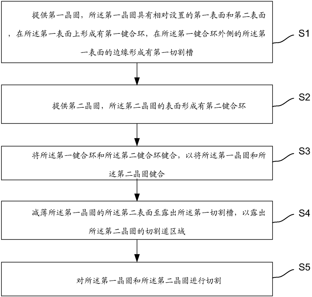
[0048] In order to solve the above-mentioned problems existing in the current technology, the invention provides a method for preparing a semiconductor device, the method comprising:

[0049] A first wafer is provided, the first wafer has a first surface and a second surface oppositely arranged, a first bonding ring is formed on the first surface, and all the outer surfaces of the first bonding ring are A first cutting groove is formed on the edge of the first surface;

[0050] providing a second wafer, the surface of the second wafer is formed with a second bonding ring;

[0051] bonding the first bonding ring to the second bonding ring to bond the first wafer to the second wafer;

[0052] thinning the second surface of the first wafer to expose the first dicing groove and simultaneously exposing the dicing groove region of the second wafer;

[0053] cutting the first wafer and the second wafer.

[0054] Specifically, the widths of the dicing lines on the outside of the fi...

Embodiment 1

[0069] The preparation method of the semiconductor device of the present invention is described in detail below with reference to the accompanying drawings, figure 1 Shows a flow chart of the fabrication process of the semiconductor device of the present invention; Figures 2A-2H A schematic cross-sectional view of a structure obtained by implementing the method for manufacturing a semiconductor device according to an embodiment of the present invention is shown.

[0070] The invention provides a method for preparing a semiconductor device, such as figure 1 As shown, the main steps of the preparation method include:

[0071] Step S1: providing a first wafer, the first wafer has a first surface and a second surface oppositely arranged, a first bonding ring is formed on the first surface, and a first bonding ring is formed on the first bonding ring A first cutting groove is formed on the edge of the first surface on the outer side;

[0072] Step S2: providing a second wafer, ...

Embodiment 2

[0134] The present invention also provides a semiconductor device, which is prepared by the method described in the first embodiment.

[0135] The semiconductor device includes:

[0136] first wafer;

[0137] a first dicing groove and a second dicing groove located in the first wafer;

[0138] A second wafer, where the second wafer is integrated with the first wafer.

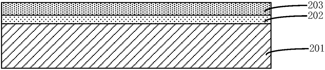
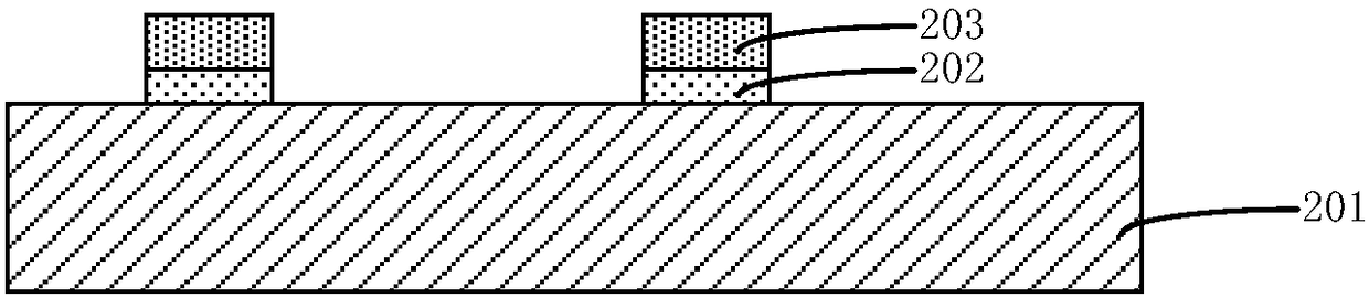
[0139] The first wafer 201 may be at least one of the materials mentioned below: silicon, silicon-on-insulator (SOI), silicon-on-insulator (SSOI), silicon-germanium-on-insulator (S-SiGeOI) and Silicon germanium on insulator (SiGeOI), etc.

[0140] In the present invention, the semiconductor device can be a MEMS device, the first wafer 201 is a cover wafer, the second wafer is a MEMS wafer, and pressure sensors and acceleration sensors can be formed on the MEMS wafer. , CMOS image sensors, etc., as well as conventional devices such as active devices, other MEMS devices, and interconnect structures.

[0141] ...


PUM

PropertyMeasurementUnit
widthaaaaaaaaaa

Abstract

The invention relates to a semiconductor device and a preparation method thereof, and an electronic apparatus. The method comprises the following steps: providing a first wafer, wherein the first wafer has a first surface and a second surface, which are arranged to be opposite to each other, a first bonding ring is formed on the first surface, and a first scribe lane is formed on the edge of the first surface on the outer side of the first bonding ring; providing a second wafer, wherein a second bonding ring is formed on the surface of the second wafer; bonding the first bonding ring with thesecond bonding ring to bond the first wafer with the second wafer; thinning the second surface of the first wafer to expose the first scribe lane so as to expose a cutting channel area of the second wafer; and cutting the first wafer and the second wafer. The preparation method provided by the invention has the advantages of: 1. simplifying the cutting process (blind dicing and multiple alignmentoperations are omitted), reducing the cutting frequency, and effectively reducing the process cost.

Description

technical field [0001] The invention relates to the technical field of semiconductors, in particular to a semiconductor device, a preparation method, and an electronic device. Background technique [0002] In the field of electronic consumption, multi-function devices are more and more popular among consumers. Compared with devices with simple functions, the production process of multi-function devices will be more complicated, such as the need to integrate multiple chips with different functions on the circuit board, so 3D integrated circuit (integrated circuit, IC) technology is defined, and 3D integrated circuit (integrated circuit, IC) is defined as a system-level integrated structure, where multiple chips are stacked in a vertical plane direction, thereby saving space. [0003] With the development of 3D IC technology, MEMS products are becoming more and more abundant, and some products still use traditional technology, adding some test patterns (test keys) in the scrib...

Claims


Application Information

Patent Timeline
Patent Type & Authority Applications(China)
IPC IPC(8): B81C3/00
CPCB81C3/001B81C2203/0785B81C2203/0792
Inventor 陆建刚陈福成
Owner SEMICON MFG INT (SHANGHAI) CORP
Why Eureka
Try Eureka