Conductor structure, capacitor array structure and preparation method

A capacitor structure and conductor structure technology, which is applied in semiconductor/solid-state device manufacturing, circuits, transistors, etc., can solve the problems of limited polysilicon crystal grain size and increased conductivity.

Active Publication Date: 2018-06-12
CHANGXIN MEMORY TECH INC
View PDF13 Cites 11 Cited by
  • Summary
  • Abstract
  • Description
  • Claims
  • Application Information

AI Technical Summary

Problems solved by technology

[0005] In view of the shortcomings of the prior art described above, the purpose of the present invention is to provide a conductor structure based on polysilicon process, a capacitor array structure and their respective prep

Method used


Image

  • Conductor structure, capacitor array structure and preparation method
  • Conductor structure, capacitor array structure and preparation method
  • Conductor structure, capacitor array structure and preparation method

Examples


Embodiment 1

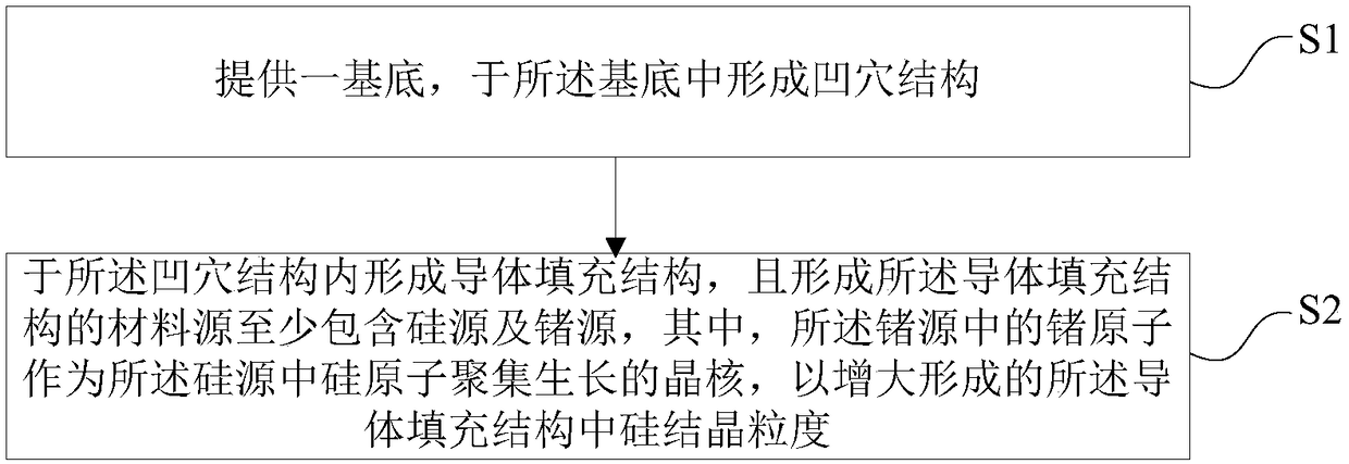
[0115] Such as Figure 1~4 As shown, the present invention provides a method for preparing a conductor structure based on a polysilicon process, comprising the steps of:

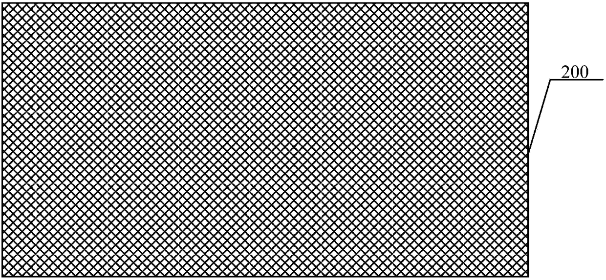
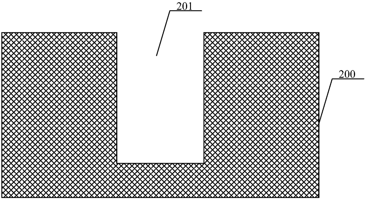
[0116] First, if figure 1 S1 and Figure 2~3 As shown, step 1) is performed, a substrate 200 is provided, and the cavity structure 201 is formed in the substrate 200 .

[0117] Specifically, this step provides a structural basis for subsequent formation of a conductor filling structure, wherein the substrate 200 can be a single material layer, such as a silicon material layer, a silicon-on-insulator material layer, a germanium material layer, and an insulating dielectric layer (such as silicon oxide Layer) etc. are used to open trenches therein and form a conductor filling structure as a metal connection line. Of course, the substrate 200 can also be any semiconductor stacked structure, and it is necessary to open a cavity therein for preparing a conductor filling structure to realize The role of conducti...

Embodiment 2

[0158] Such as Figure 5 As shown, the present invention also provides a method for preparing a capacitor structure array, wherein the preparation of the capacitor structure array in the second embodiment includes the preparation of the conductor structure based on the polysilicon process in the first embodiment, including steps:

[0159] 1) A semiconductor substrate is provided, the semiconductor substrate includes a plurality of capacitive contact nodes located in the memory array structure, and alternately stacked sacrificial layers and supporting layers are formed on the semiconductor substrate;

[0160] 2) forming a patterned mask layer with windows arranged in an array on the structure obtained in step 1), and etching the sacrificial layer and the supporting layer based on the patterned mask layer to form a a capacitive hole corresponding to the window, the capacitive hole exposing the capacitive contact node;

[0161] 3) forming a lower electrode layer on the bottom an...


PUM

PropertyMeasurementUnit
Thicknessaaaaaaaaaa

Abstract

The invention provides a conductor structure based on a polysilicon process, a capacitor array structure and a preparation method. The preparation method of the conductor structure comprises the stepsthat a substrate is provided, and a recess structure is formed in the substrate; a conductor filling structure is formed in the recess structure, and a material source which forms the conductor filling structure at least comprises a silicon source and a germanium source; and germanium atoms in the germanium source serve as crystal nucleuses for aggregating and growing silicon atoms in the siliconsource to increase the silicon crystal grain size in the conductor filling structure. According to the scheme provided by the invention, the method of manufacturing large-grain polycrystalline silicon is proposed; the crystal nucleus element for aggregating and growing silicon crystal grains is introduced, such as germanium, so that silicon atoms are aggregated to increase the crystal grain size;increasing the crystal grain size of polycrystalline silicon can reduce the influence of grain boundary traps on carriers and further increases the conductivity; a protective layer is arranged to prevent the influence of germanium in the conductor filling structure on the process; and the conductor filling structure and other structural layers are effectively connected, which further improves theelectrical properties of the conductor filling structure.

Description

technical field [0001] The invention belongs to the field of semiconductor devices and manufacturing, and in particular relates to a conductor structure based on a polysilicon process, a capacitor array structure and a preparation method. Background technique [0002] Dynamic Random Access Memory (DRAM for short) is a semiconductor storage device commonly used in computers, and is composed of many repeated storage units. Each memory cell usually includes a capacitor and a transistor; the gate of the transistor is connected to the word line, the drain is connected to the bit line, and the source is connected to the capacitor; the voltage signal on the word line can control the opening or closing of the transistor, and then through the bit line Read the data information stored in the capacitor, or write the data information into the capacitor through the bit line for storage. At present, in the DRAM process below 20nm, the DRAM adopts a stacked capacitor structure, and its ca...

Claims


Application Information

Patent Timeline
IPC IPC(8): H01L21/8242H01L27/108
CPCH10B12/37H10B12/03
Inventor 不公告发明人
Owner CHANGXIN MEMORY TECH INC
Why Eureka
Try Eureka