Atomic bonding-based on-chip microflow cooling GaN crystal tube and manufacturing method thereof

A technology of transistors and gallium nitride, which is applied in the direction of electrical solid-state devices, semiconductor devices, semiconductor/solid-state device components, etc., can solve problems such as limiting the performance of gallium nitride devices, low thermal conductivity, and degradation of device performance and reliability. Achieve the effect of improving high-efficiency heat dissipation characteristics and high-efficiency heat dissipation capabilities

Active Publication Date: 2018-06-15
NO 55 INST CHINA ELECTRONIC SCI & TECHNOLOGYGROUP CO LTD
View PDF7 Cites 7 Cited by
  • Summary
  • Abstract
  • Description
  • Claims
  • Application Information

AI Technical Summary

Problems solved by technology

This is mainly because high-power microwave devices will generate a large amount of heat accumulation while outputting high power, especially for microwave power devices with an output power of hundreds of watts or even thousands of watts, which will cause a sharp rise in the junction temperature of the device and cause its device Severe degradation in performance and reliability
[0003] At present, GaN-based power devices are mainly epitaxially grown on substrate materials such as silicon carbide and sapphire, and these substrate materials have low thermal conductivity. The heat dissipation problem ser

Method used


Image

  • Atomic bonding-based on-chip microflow cooling GaN crystal tube and manufacturing method thereof
  • Atomic bonding-based on-chip microflow cooling GaN crystal tube and manufacturing method thereof
  • Atomic bonding-based on-chip microflow cooling GaN crystal tube and manufacturing method thereof

Examples


Example Embodiment

[0033] Example

[0034] A method for designing and manufacturing a near-junction microflow embedded gallium nitride transistor with high efficiency heat dissipation, including:

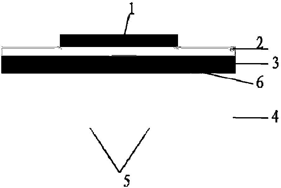
[0035] 1) Complete the conventional front-side process of gallium nitride transistors to obtain gallium nitride transistors, the substrate of which is made of SiC material, the size of the active region is 60*125um, and it is a two-gate structure;

[0036] 2) In-chip microfluidic channel preparation based on atomic bonding;

[0037] ① Coating a layer of silicon oxide dielectric protective layer on the front of the completed gallium nitride transistor to protect the functional area, and using bonding technology to bond the front of the transistor to the temporary carrier;

[0038] ② Put the gallium nitride transistor containing the temporary carrier into the grinding machine, and grind and thin the SiC substrate to a thickness of 15 microns;

[0039] ③ Coat one side of a new SiC substrate with a sili...


PUM


Abstract

The invention discloses an atomic bonding-based on-chip microflow cooling GaN crystal tube and a manufacturing method thereof. The GaN crystal tube sequentially comprises an active region functional layer, a barrier layer, a buffer layer and a substrate from top to bottom, wherein a micro fluid passage is arranged in the substrate, is arranged below the active region functional layer and is formedby an atomic bonding process, and a micro fluid is arranged in the micro fluid passage. A fluid cooling technology is introduced to a chip by the atomic bonding technology, atomic bonding employs anoxide or nitride medium, the thickness of a bonding layer is several nanometers, the thermal resistance of the bonding package layer is effectively reduced, the high-efficiency cooling performance ofthe chip is achieved, and heat accumulation of the large-power GaN device is solved; and compared with a traditional GaN device, the GaN crystal tube has the advantages that the power density can be improved by over two times, the maximum output power of the device is greatly improved, and relatively high reliability is maintained.

Description

technical field [0001] The invention belongs to the technical field of thermal management development of power devices, in particular to an atomic-bonding-based on-chip microfluidic heat dissipation gallium nitride transistor and a manufacturing method thereof. technical background [0002] The third-generation semiconductor power devices represented by GaN have demonstrated their excellent high-power application characteristics. In practical applications, GaN power chips are mostly SiC substrates, and the power density of their power devices has only reached its theoretical level. One-fifth of the value, GaN's high-power characteristics are far from being brought into play. This is mainly because high-power microwave devices will generate a large amount of heat accumulation while outputting high power, especially for microwave power devices with an output power of hundreds of watts or even thousands of watts, which will cause a sharp rise in the junction temperature of the ...

Claims


Application Information

Patent Timeline
IPC IPC(8): H01L23/46H01L23/473
CPCH01L23/46H01L23/473
Inventor 郭怀新孔月婵吴立枢黄宇龙陈堂胜
Owner NO 55 INST CHINA ELECTRONIC SCI & TECHNOLOGYGROUP CO LTD
Why Eureka
Try Eureka