Polycrystal black silicon texturing process

A technology of black silicon and process, which is applied in the field of polycrystalline black silicon texturing process, can solve the problems of complex texturing process and lack of silicon wafers, etc., and achieve the effect of uniform holes, blurred appearance and good appearance

Active Publication Date: 2018-06-22
CHANGZHOU SHICHUANG ENERGY CO LTD
View PDF5 Cites 11 Cited by
  • Summary
  • Abstract
  • Description
  • Claims
  • Application Information

AI Technical Summary

Problems solved by technology

However, the process of metal ion-induced black silicon texturing is complicated. If the control is not good, silicon wafers with good appearance and high efficiency cannot be obtained.

Method used


Image

  • Polycrystal black silicon texturing process
  • Polycrystal black silicon texturing process

Examples


Embodiment 1

[0036] A polycrystalline black silicon texturing process, comprising the steps of:

[0037] 1) Polysilicon wafers are polished with polishing liquid;

[0038] The polishing liquid is composed of 5% to 15% potassium hydroxide or sodium hydroxide, 0.3% to 0.8% polishing auxiliary agent and the balance of deionized water;

[0039] The polishing aid is composed of 1.0% to 3.0% sodium benzoate, 1.0% to 2.0% sodium acetate, 0.5% to 2.0% glycerol, 0.2% to 1.0% polyethylene glycol, 5.0% to 10.0% sodium silicate and The remainder is composed of deionized water;

[0040] The temperature of the polishing treatment is 70-80°C, and the time is 200-250s;

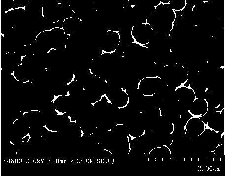
[0041] 2) Dig holes on the polished silicon wafers with a hole-digging treatment solution, and prepare nano-holes on the surface of the silicon wafers;

[0042] The hole-digging treatment liquid is composed of 0.2%-0.5% hydrogen peroxide, 2%-5% hydrofluoric acid, 0.4%-1.2% hole-digging auxiliary agent and the balance of deionized water...

Embodiment 2

[0051] On the basis of embodiment 1, the difference is:

[0052] The polishing liquid is composed of 8% to 12% potassium hydroxide or sodium hydroxide, 0.4% to 0.7% polishing auxiliary agent and the balance of deionized water;

[0053] The polishing aid consists of 1.5% to 2.0% sodium benzoate, 1.5% to 2.0% sodium acetate, 1.0% to 2.0% glycerol, 0.5% to 0.8% polyethylene glycol, 5.0% to 8.0% sodium silicate and The remainder is composed of deionized water;

[0054] Wherein, each percentage is volume percentage.

Embodiment 3

[0056] On the basis of embodiment 1, the difference is:

[0057]The hole-digging treatment liquid is composed of 0.2%-0.4% hydrogen peroxide, 2%-4% hydrofluoric acid, 0.5%-1.0% hole-digging auxiliary agent and the balance of deionized water;

[0058] The hole-digging auxiliary agent consists of 1.0%-2.0% citric acid, 1.0%-2.0% butanediol, 0.05%-0.1% silver nitrate, 0.2%-0.5% hydroxyethyl cellulose, 1.5%-3.0% tartaric acid, 0.5%~0.8% polyethylene glycol, 0.5%~0.8% silane coupling agent, 0.8%~1.0% triethanolamine, 0.5%~0.8% polyaspartic acid, 0.5%~1.0% polyvinyl alcohol, 0.5% ~1.0% polyoxyethylene lauryl ether and the balance of deionized water;

[0059] Wherein, each percentage is volume percentage.


PUM


Abstract

The invention discloses a polycrystal black silicon texturing process. The polycrystal black silicon texturing process includes the following steps that 1), a polycrystalline silicon wafer is polishedthrough polishing liquid; 2), the polished silicone wafer is hole-dug through hole-digging treating liquid, and nano-holes are prepared in the surface of the silicone wafer; 3), the hole-dug siliconewafer is de-silverized, and silver particles on the silicone wafer are removed; 4), the de-silverized silicone wafer is chambered through chambering treating liquid, and micro-nano holes are preparedin the surface of the silicone wafer. According to the polycrystal black silicon texturing process, by means of control over the three key steps of polishing, hole-digging and chambering, the whole black silicone texturing process is controllable, polycrystal black silicon with the good appearance and high efficiency can be prepared, and the prepared polycrystal black silicon is fuzzy in appearance and is provided with uniform holes.

Description

technical field [0001] The invention relates to a polycrystalline black silicon texturing process. Background technique [0002] Since the cutting cost of diamond wire-cut polysilicon wafers is 0.3-0.7 yuan lower than that of mortar wafers, there is an urgent desire to switch from mortar multi-wafers to diamond wire multi-wafers in the market. However, the texturing of diamond wire polysilicon wafers is a big problem. Due to the shallow damage layer cut by diamond wire polysilicon wafers, the difference between the line mark area and the non-line mark area is large, and the reflection and line marks on the surface of the silicon wafer after conventional acid texturing are serious, the cashmere rate is low, and the reflectivity is high, so After being made into a battery sheet, the efficiency is low, and the appearance cannot pass. [0003] At present, the methods that can be solved include additive texturing, metal ion induced black silicon texturing, RIE black silicon tex...

Claims


Application Information

Patent Timeline
Patent Type & Authority Applications(China)
IPC IPC(8): C30B33/10C30B29/06
CPCC30B29/06C30B33/10
Inventor 章圆圆裴银强常振宇陈其成
Owner CHANGZHOU SHICHUANG ENERGY CO LTD
Why Eureka
Try Eureka