Semiconductor structure and formation method thereof

A technology of semiconductor and gate structure, which is applied in the field of semiconductor structure and its formation, can solve the problems of high process cost, achieve the effect of increasing the driving current, reducing the contact resistance, and having little influence

Active Publication Date: 2018-07-06
SEMICON MFG INT (SHANGHAI) CORP +1
View PDF7 Cites 7 Cited by
  • Summary
  • Abstract
  • Description
  • Claims
  • Application Information

AI Technical Summary

Problems solved by technology

[0005] Although the DSS implantation process can effectively reduc

Method used


Image

  • Semiconductor structure and formation method thereof
  • Semiconductor structure and formation method thereof
  • Semiconductor structure and formation method thereof

Examples


Embodiment Construction

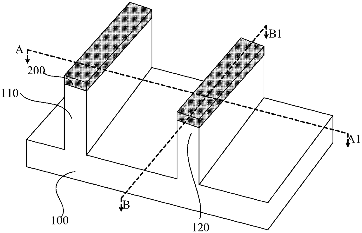
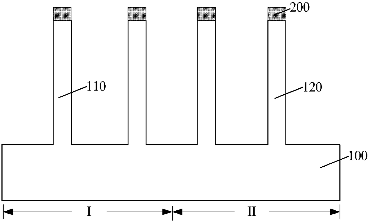
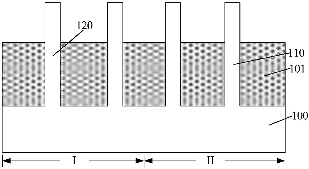
[0015] It can be known from the background art that although the Dopant Segregated Schottky (DSS) implantation process can effectively reduce the Schottky barrier height, the process cost is relatively high. Analyze the reasons for this:

[0016] During the DSS implantation process, the type of ions implanted in the source and drain doped regions of the N-type region is different from the ion type implanted in the source and drain doped regions of the P-type region. During DSS implantation, the implanted ion source used is P or As, and when the P-type DSS implantation is performed on the source and drain doped regions of the P-type region, the implanted ion source used is B or BF 2 Therefore, two photomasks are required to perform the N-type DSS injection and the P-type DSS injection respectively, and the process cost is relatively large.

[0017] In order to solve the above technical problem, the present invention provides a method for forming a semiconductor structure. In t...


PUM


Abstract

Disclosed are a semiconductor structure and a formation method thereof. The formation method comprises the steps of forming a base, wherein the base comprises a substrate, a gate structure positionedon the substrate, source and drain doped regions positioned in the base on the two sides of the gate structure, and an interlayer dielectric layer positioned on the base and for covering the top of the gate structure, and the substrate comprises a first region for forming a P type device and a second region for forming an N type device; forming a first contact opening for exposing the source and drain doped regions in the interlayer dielectric layer on the two sides of the gate structure; performing a P type dopant segregated schottky doping process on the source and drain doped regions exposed from the first contact opening in the first region and the second region; forming a metal silicide layer at the bottom of the first contact opening; and forming a first contact hole inserting plug in the first contact opening. By adjusting the doping concentration of the source and drain doped regions in the second region, use of a photomask can be avoided when the P type dopant segregated schottky doping process is performed, so that lowering of the process cost is realized, and the N type device suffers from relatively low influence.

Description

technical field [0001] The invention relates to the field of semiconductors, in particular to a semiconductor structure and a forming method thereof. Background technique [0002] With the continuous development of integrated circuit manufacturing technology, the critical dimensions of devices are getting smaller and smaller, and many problems have arisen accordingly. For example, the contact resistance between the contact hole plug and the source-drain doped region increases, which leads to a decrease in the response speed of the device, a delay in the signal, and a decrease in the driving current, thereby degrading the performance of the semiconductor device. [0003] In order to reduce the contact resistance between the contact hole plug and the source-drain doped region, a metal silicide process is introduced. The metal silicide has a lower resistivity and can significantly reduce the contact resistance, thereby increasing the driving current. [0004] With the continuo...

Claims


Application Information

Patent Timeline
IPC IPC(8): H01L21/8238H01L27/092
CPCH01L21/823814H01L21/823821H01L21/823871H01L27/0924
Inventor 李勇
Owner SEMICON MFG INT (SHANGHAI) CORP
Why Eureka
Try Eureka