Zinc indium tin oxide-based film transistor and manufacturing method thereof
A thin-film transistor and oxide-based technology, applied in the field of electronic information, can solve the problems of low mobility and high preparation temperature of thin-film transistors
- Summary
- Abstract
- Description
- Claims
- Application Information
AI Technical Summary
Problems solved by technology
Method used
Image
Examples
Embodiment 1
[0070] The embodiment of the present invention provides a zinc indium tin oxide based thin film transistor and its manufacturing method, which is composed of Zn x In y sn z O:(Li a ,N b ) material to prepare the active layer, use SiO 2 And the high-k material is used as an insulating layer to obtain a transparent thin film transistor. The problems of low mobility of commercial thin film transistors and high preparation temperature of high mobility thin film transistors are solved.
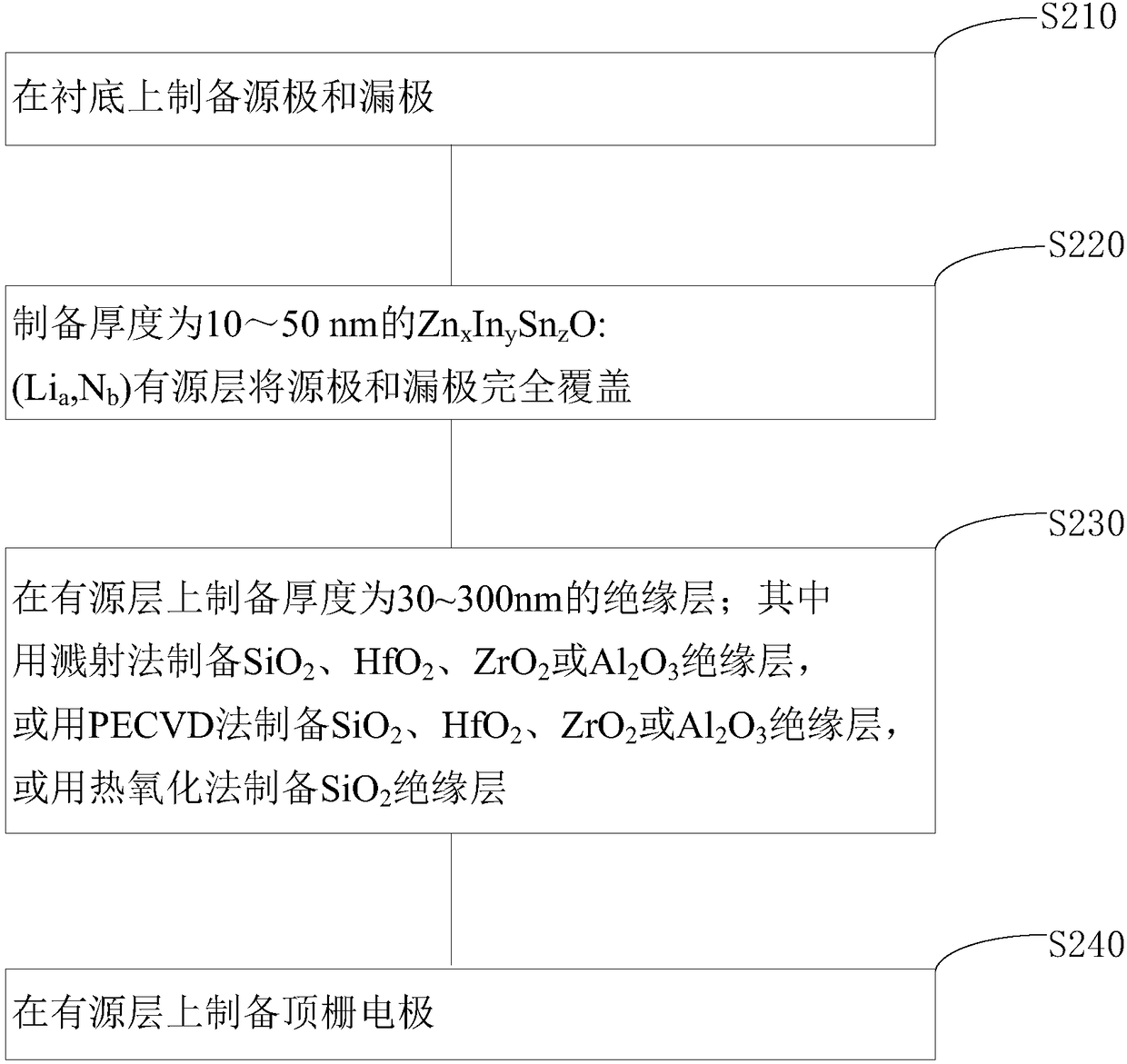
[0071] One aspect of the present invention provides a method for manufacturing a zinc indium tin oxide based thin film transistor.
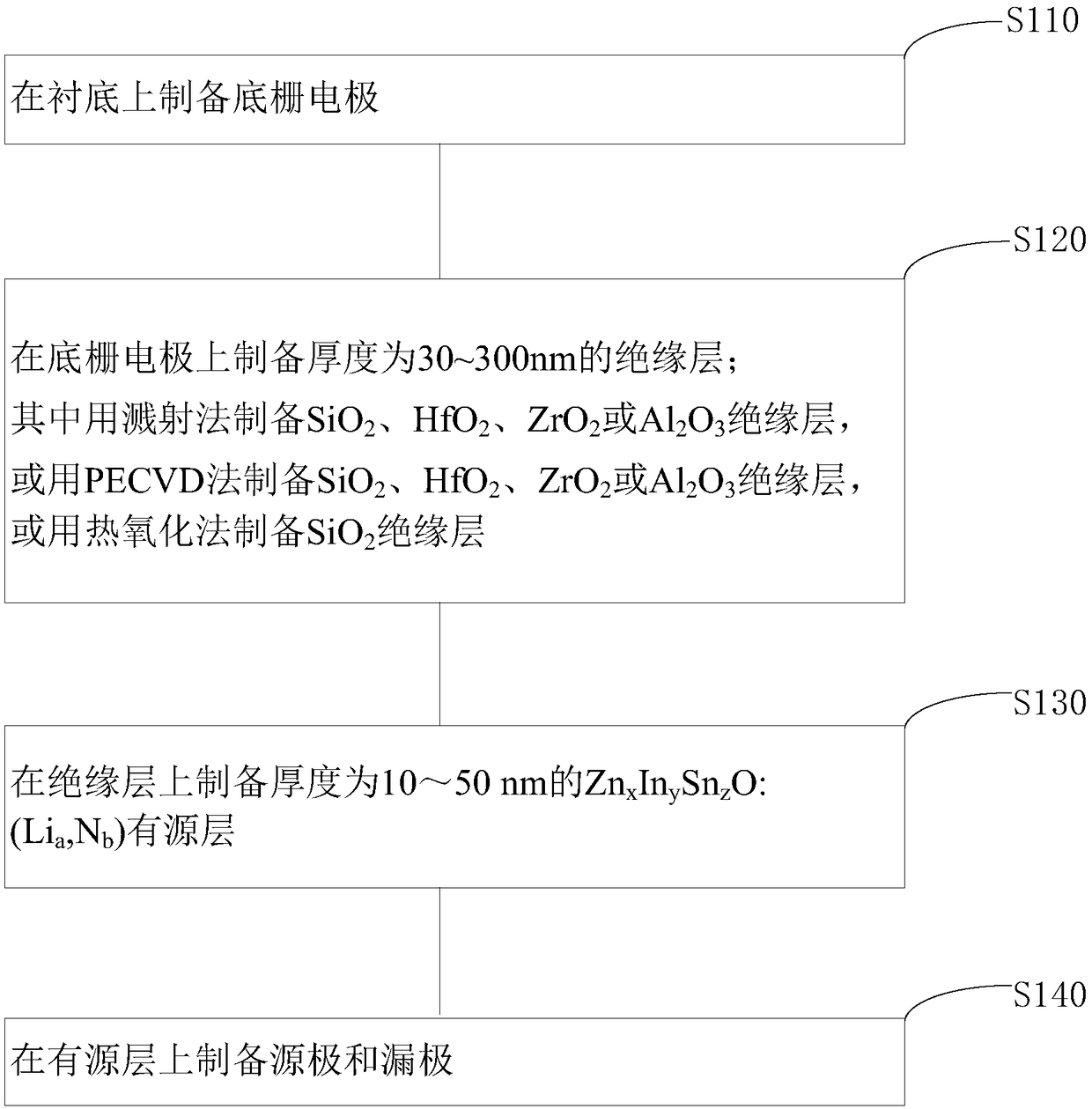
[0072] The processing flow of a method for manufacturing a zinc indium tin oxide-based thin film transistor provided in an embodiment of the present invention is as follows: figure 1 As shown, the following processing steps are included:
[0073] Step S110: preparing a bottom gate electrode on the substrate.
[0074] On a glass substrate, the bottom gate elect...
Embodiment 2
[0105] This embodiment provides a method for manufacturing a zinc indium tin oxide-based thin film transistor, and its specific implementation steps are as follows:
[0106] Step 1: preparing an ITO bottom gate on a glass substrate.
[0107] Step 2: Prepare an insulating layer on the electrode prepared in step 1, and grow the insulating layer as HfO 2 , with a thickness of 30nm.
[0108] Step 3: Prepare Zn by magnetron sputtering x In y sn z O:(Li a ,N b ) active layer, the thickness is 10nm, x=0.1, y=2, z=0.01, a=0.1, b=0, the sputtering power is 75W, the oxygen / argon pressure ratio is 30%, the growth temperature is room temperature, no annealing.
[0109] Step 4: Prepare Ti / Au source and drain electrodes by magnetron sputtering.
[0110] Produce ITO / HfO 2 / Zn x In y sn z O:(Li a ,N b ) / Ti / Au bottom gate structure zinc indium tin oxide based thin film transistor.
Embodiment 3
[0112] This embodiment provides a method for manufacturing a zinc indium tin oxide-based thin film transistor, and its specific implementation steps are as follows:
[0113] Step 1: On the Si substrate, prepare SiO by thermal oxidation 2 The insulating layer has a thickness of 200 nm.
[0114] Step 2: Prepare Zn on the SiO2 insulating layer by magnetron sputtering x In y sn z O:(Li a ,N b ) active layer, the thickness is 20nm, x=1, y=1.1, z=0.1, a=0.01, b=0, sputtering power is 100W, oxygen / argon pressure ratio is 0%, growth temperature is room temperature, annealing The temperature is 320° C., and the annealing atmosphere is nitrogen.
[0115] Step 3: Prepare Al source, drain and bottom gate by thermal evaporation.
[0116] Produced Al / Si / SiO 2 / Zn x In y sn z O:(Li a ,N b ) / Al bottom gate structure zinc indium tin oxide based thin film transistor.
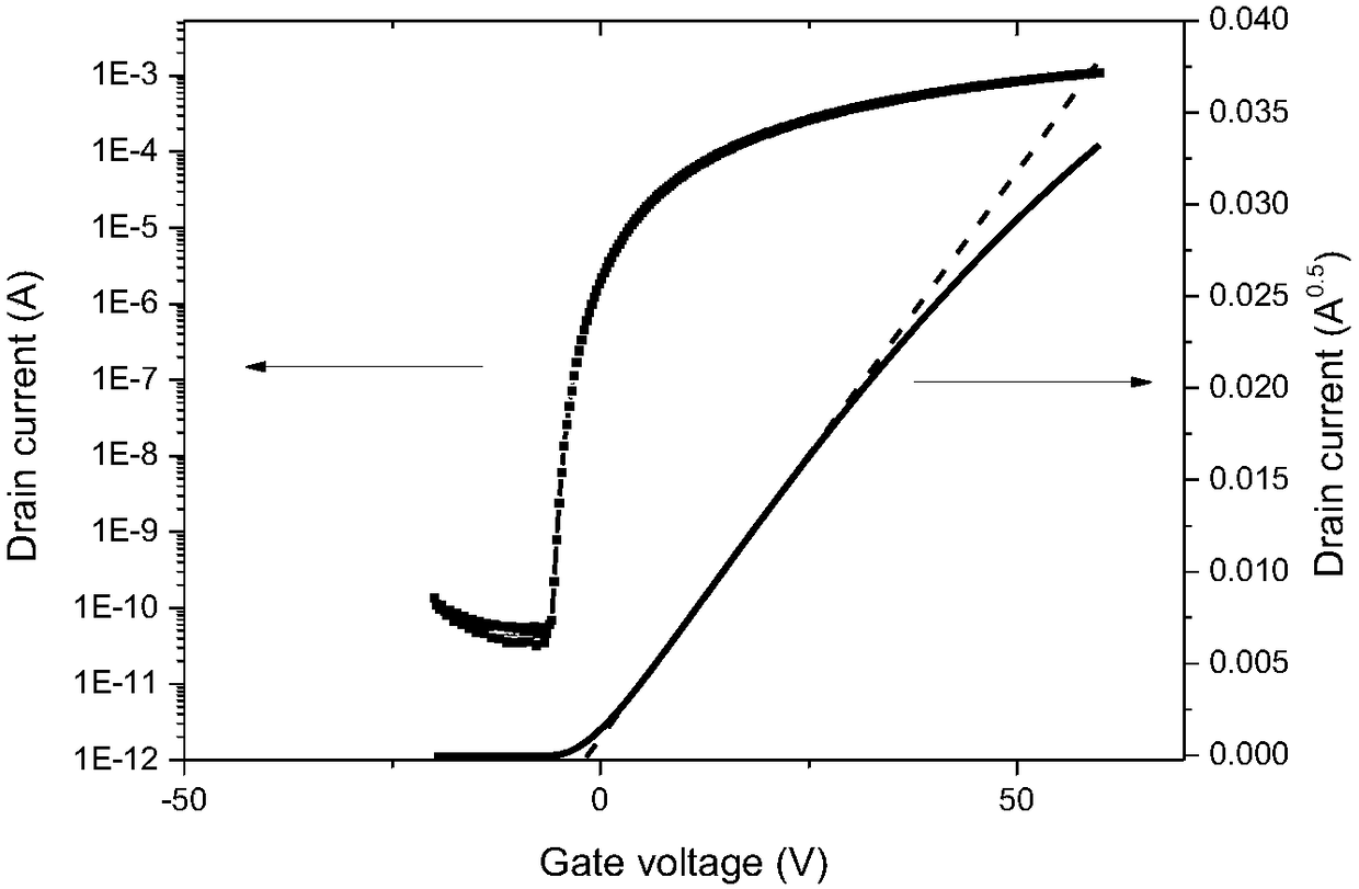
[0117] Zn produced by the above-mentioned production method two x In y sn z O:(Li a ,N b ) thin film transis...
PUM
| Property | Measurement | Unit |
|---|---|---|
| Thickness | aaaaa | aaaaa |
| Thickness | aaaaa | aaaaa |
| Thickness | aaaaa | aaaaa |
Abstract
Description
Claims
Application Information
 - R&D
- Intellectual Property
- Life Sciences
- Materials
- Tech Scout
- Unparalleled Data Quality
- Higher Quality Content
- 60% Fewer Hallucinations
Browse by: Latest US Patents, China's latest patents, Technical Efficacy Thesaurus, Application Domain, Technology Topic, Popular Technical Reports.
© 2025 PatSnap. All rights reserved.Legal|Privacy policy|Modern Slavery Act Transparency Statement|Sitemap|About US| Contact US: help@patsnap.com


