An electron beam excited fluorescence large-scale direct detection imaging device and method thereof

An imaging device and electron beam technology, applied in measuring devices, photometry, photometry using electric radiation detectors, etc., can solve complex operations, increase system complexity and operational convenience, and spectral signal distortion, etc. question

Active Publication Date: 2019-07-26
北京金竟科技有限责任公司
View PDF8 Cites 2 Cited by
  • Summary
  • Abstract
  • Description
  • Claims
  • Application Information

AI Technical Summary

Problems solved by technology

[0005] Usually, the electron beam excited fluorescence signal is generated in the vacuum sample chamber. The fluorescence signal needs to be transmitted from the inside of the vacuum sample chamber to the fluorescence intensity or spectrum detection system outside the vacuum sample chamber. During the transmission of the fluorescence signal, it is easy to cause the attenuation of the fluorescence intensity and the The signal is distorted, and the overall system configuration is cumbersome, and the operation is relatively complicated
For example, when using a photomultiplier tube for fluorescence intensity detection, since the overall size of the photomultiplier tube is usually larger than 10-30 mm, and requires about 1,000 volts of DC high voltage to work, it is difficult to integrate into the scanning electron microscope system due to the influence of size and electromagnetic interference In the vacuum sample chamber, the fluorescence signal can only be detected through the fluorescence signal transmission optical path inside the vacuum sample chamber; when the fluorescence signal is transmitted through the fluorescence signal transmission optical path, due to the coupling efficiency and the Due to the absorption effect, the fluorescence signal intensity will be attenuated by more than 20%, which reduces the detection efficiency of the fluorescence intensity; and the photomultiplier tube and its detection circuit loaded outside the scanning electron microscope system need additional installation and configuration, which increases the complexity of the system and ease of operation

Method used


Image

  • An electron beam excited fluorescence large-scale direct detection imaging device and method thereof
  • An electron beam excited fluorescence large-scale direct detection imaging device and method thereof
  • An electron beam excited fluorescence large-scale direct detection imaging device and method thereof

Examples


Embodiment Construction

[0031] The present invention will be further described through the embodiments below in conjunction with the accompanying drawings.

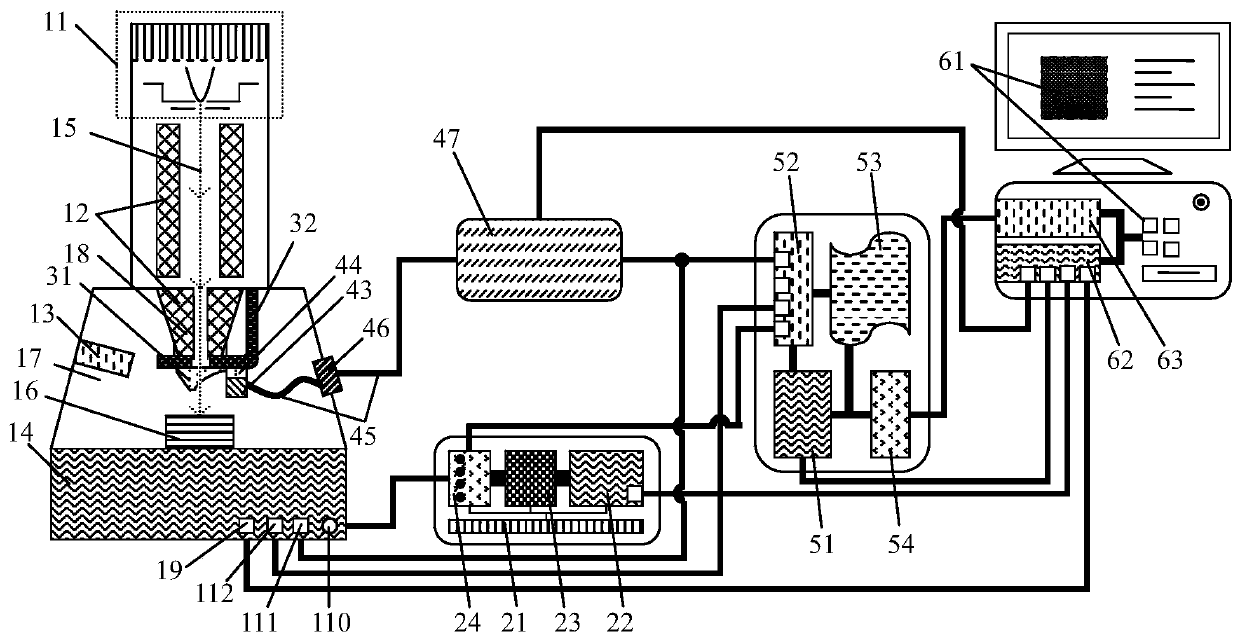
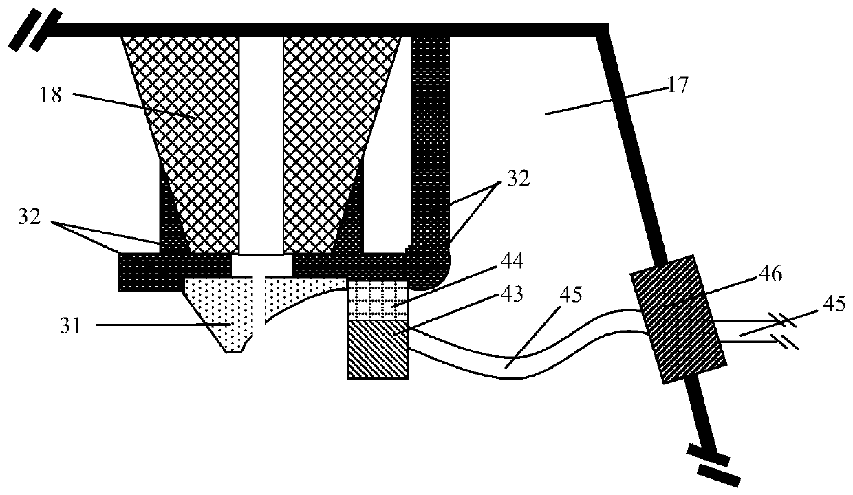
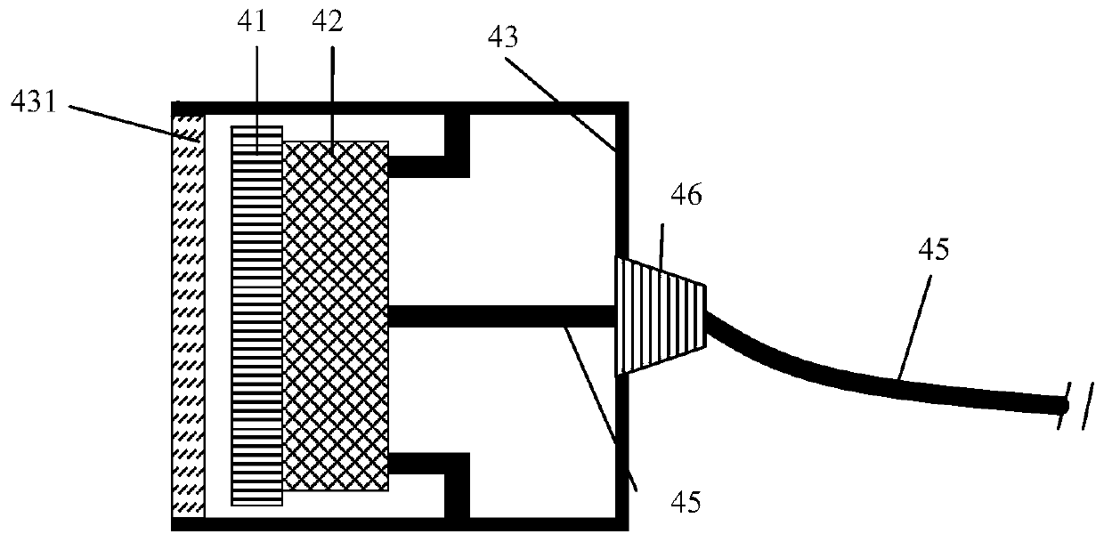
[0032] Such as figure 1 As shown, the electron beam excited fluorescence large-scale direct detection imaging device of this embodiment includes: a scanning electron microscope system, a scanning signal generator, a fluorescence collection and coupling system, a semiconductor photodetector, a scanning synchronous signal acquisition device, cooperative control and data processing Output system; wherein, the collaborative control and data processing output system is used as a synchronous control and data acquisition center, and is connected to the scanning electron microscope system, scanning signal generator, semiconductor photodetector and scanning synchronous signal collector; the scanning signal generator is also connected to The external scanning control interface of the electron beam to the scanning electron microscope system; the fluorescen...


PUM


Abstract

The invention discloses an electron beam excitation fluorescence large-range direct detection imaging apparatus and a method thereof. The imaging apparatus comprises a scanning electron microscope system, a scanning signal generator, a fluorescence collection coupling system, a semiconductor photodetector, a scanning synchronization signal collector and a synergic control and data processing output system. According to the present invention, by using the modular architecture, the configuration adjustment and the subsequent upgrade of each module are flexible and convenient; and by introducingthe large-area semiconductor photoelectric detection chip of the semiconductor photodetector, the fluorescence excited by the scanning electron microscope system in the large imaging visual field range can be concentrated and coupled to the semiconductor photodetector at the same high collection efficiency, such that the problem that the fluorescence excitation intensities or the fluorescence excitation yields at different positions of the image obtained through the large-range fluorescence scanning imaging are difficultly calculated and compared by using the standard is solved so as to complete the large-range rapid detection and analysis based on the electron beam excitation fluorescence signals.

Description

technical field [0001] The invention relates to the detection and processing technology of fluorescence signals excited by electron beams, in particular to an imaging device and method for direct detection and imaging of large-scale fluorescence excited by electron beams. Background technique [0002] The fluorescent signal excited by the electron beam refers to the electromagnetic waves emitted by the electron beam in the ultraviolet, infrared or visible light band except for secondary electrons, backscattered electrons, Auger electrons and X-rays when the electron beam bombards the surface of the material; The basic principle is that the electrons inside the material are excited by the incident electrons to a high-energy state, and after a certain relaxation time, they transition back to a low-energy state and release energy, and part of the energy is emitted in the form of electromagnetic radiation. The physical process of a material producing fluorescence under electron ...

Claims


Application Information

Patent Timeline
Patent Type & Authority Patents(China)
IPC IPC(8): G01N23/2251G01J1/42G01J1/04
CPCG01J1/0422G01J1/0455G01J1/0459G01J1/42G01J2001/4242G01N23/2251G01N2223/07G01N2223/102G01N2223/507
Inventor 朱瑞徐军刘亚琪
Owner 北京金竟科技有限责任公司
Why Eureka
Try Eureka