Silicon carbide power device having step structure and fabrication method of silicon carbide power device

A power device, silicon carbide technology, applied in semiconductor/solid-state device manufacturing, semiconductor devices, electrical components, etc., can solve the problems of N-type SiC surface doping characteristics change, affecting low device turn-on voltage, restricting industrialization development, etc. Achieve the effect of improving electric field concentration, high breakdown voltage, and reducing the need for complex high-temperature processes

Active Publication Date: 2018-07-13
HUNAN SANAN SEMICON CO LTD
View PDF5 Cites 15 Cited by
  • Summary
  • Abstract
  • Description
  • Claims
  • Application Information

AI Technical Summary

Problems solved by technology

Among them, epitaxial growth is to directly grow P-type SiC on the entire surface of N-type SiC layer. Since the growth temperature of P-type SiC is often high (>1500°C), some P-type impurities (such as Al) will inevitably diffuse during the growth process. In weak N-type SiC, self-doping is formed on the surface of N-type SiC, and even the area is converted into P-type, which leads to changes in the doping characteristics of the N-type SiC surface, which in turn affects the acquisition of low device turn-on voltage; P for SiC Type ion implantation often requires advanced equipment such as high-temperature ion implanters and ultra-high temperature annealing furnaces to complete, and has complex manufacturing processes and high costs, which restricts its industrial development

Method used


Image

  • Silicon carbide power device having step structure and fabrication method of silicon carbide power device
  • Silicon carbide power device having step structure and fabrication method of silicon carbide power device
  • Silicon carbide power device having step structure and fabrication method of silicon carbide power device

Examples


Embodiment 1

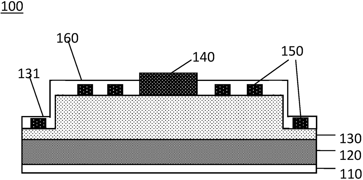
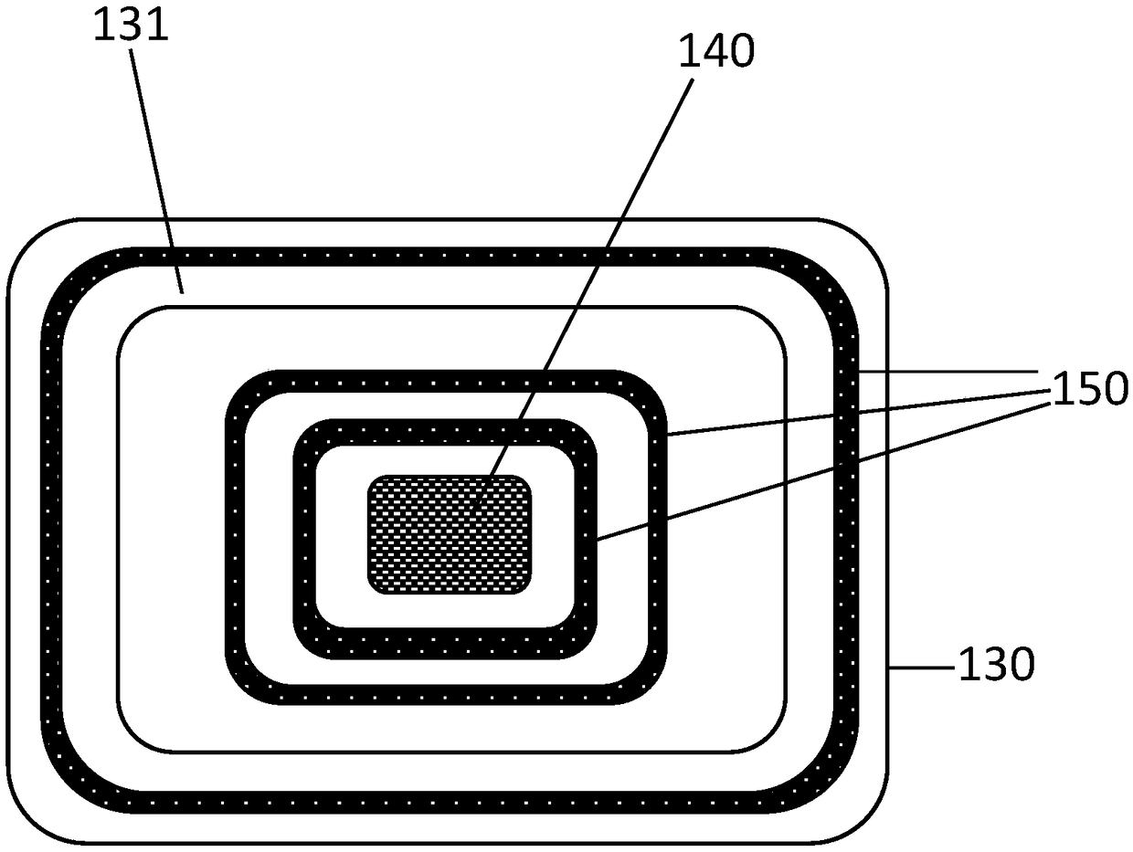
[0036] refer to figure 1 and figure 2 , a silicon carbide Schottky barrier diode (SBD) 100, comprising an ohmic contact electrode 110, N + SiC substrate layer 120, N - SiC epitaxial layer 130, Schottky contact electrode 140, P-type junction terminal 150 and passivation layer 160, ohmic contact electrode 110, N + SiC substrate layer 120 and N - The SiC epitaxial layer 130 is stacked sequentially from bottom to top, and the Schottky contact electrode 140 and the P-type junction terminal 150 are arranged on the N - On the upper surface of the SiC epitaxial layer 130, the Schottky contact electrode 140 is located in the center, and the P-type junction terminal 150 is a closed ring structure and is arranged around the periphery of the Schottky contact electrode 140 in turn. The P-type junction terminal 150 and the N - The SiC epitaxial layer 130 forms a PN heterojunction, and the passivation layer 160 covers the exposed N - SiC epitaxial layer 130 and P-type junction terminat...

Embodiment 2

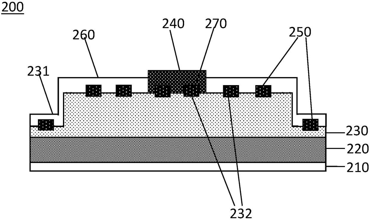
[0049] refer to image 3 , a silicon carbide junction barrier Schottky diode (JBS) 200, comprising an ohmic contact electrode 210, N + SiC substrate layer 220, N - SiC epitaxial layer 230 , Schottky contact electrode 240 , P-type junction termination 250 , passivation layer 260 and P-type structure 270 . Ohmic contact electrodes 210, N + SiC substrate layer 220 and N - The SiC epitaxial layer 230 is stacked sequentially from bottom to top, and the Schottky contact electrode 240, the P-type junction terminal 250 and the P-type structure 270 are arranged on the N - On the upper surface of the SiC epitaxial layer 230, the Schottky contact electrode 240 is located in the center, and the P-type junction terminal 250 is a closed ring structure and is arranged around the Schottky contact electrode 240 in turn. Similarly, N - The edge of the surface of the SiC epitaxial layer 230 is provided with an annular step 231, and the P-type junction terminal 250 is distributed on the upper...

Embodiment 3

[0054] refer to Figure 4 , a silicon carbide power device is a silicon carbide PN junction diode 300, including ohmic contact electrodes 310, N + SiC substrate layer 320, N - SiC epitaxial layer 330 , Schottky contact electrode 340 , P-type junction terminal 350 , passivation layer 360 and P-type layer 370 . The difference from Embodiment 2 is that the P-type layer 370 is a whole-layer structure, which is arranged between the Schottky contact electrode 340 and the N - Between the SiC epitaxial layer 330 and isolating the Schottky contact electrode 340 and the N - SiC epitaxial layer 330, P-type layer 370 and N - A PN junction is formed between the SiC epitaxial layers 330 . Likewise, N - The SiC epitaxial layer 330 is provided with an annular step 331 and a groove 332, and the P-type junction terminal 350 and the P-type layer 370 are formed in the groove 332 in one-to-one correspondence, and the P-type junction terminal 350 is distributed at the level of the annular step...


PUM


Abstract

The invention discloses a silicon carbide power device having a step structure and a fabrication method of the silicon carbide power device. The silicon carbide power device comprises an ohmic contactelectrode, an N<+>SiC substrate layer, an N<->SiC epitaxial layer and a Schottky contact electrode from bottom to top and also comprises a plurality of P-type junction terminals, wherein the Schottkycontact electrode is arranged in the center of the N<->SiC epitaxial layer, the P-type junction terminals are of closed-loop structures and are sequentially arranged around the Schottky contact electrode in an encircling way, an edge of an upper surface of the N<->SiC epitaxial layer is lower than an annular step formed in the center, the P-type junction terminals are arranged on a high step surface and a lower step surface of the annular step of the N<->SiC epitaxial layer, and the P-type junction terminals and the N<->SiC epitaxial layer form a PN heterojunction. By the silicon carbide power device, the concentration phenomenon of an edge electric field of a SiC power device junction can be improved, and the SiC power device with a high breakdown voltage is obtained.

Description

technical field [0001] The invention relates to a semiconductor device, in particular to a silicon carbide power device with a stepped structure and a preparation method thereof. Background technique [0002] Power devices based on wide-bandgap semiconductor materials (such as silicon carbide (SiC), gallium nitride (GaN)) can provide greater breakdown voltage and power density, and are expected to be widely used in next-generation power conversion. In SiC power devices, due to the discontinuity of the junction, the electric force lines tend to concentrate at the edge of the junction, resulting in the existence of a high electric field at the junction edge. The presence of a high field will lead to premature breakdown at the junction edge, which greatly limits the reverse breakdown voltage of the device. Therefore, in the design and manufacture of SiC power devices, various junction termination technologies are often used to alleviate the edge electric field concentration ef...

Claims


Application Information

Patent Timeline
Patent Type & Authority Applications(China)
IPC IPC(8): H01L29/872H01L29/06H01L21/329
CPCH01L29/0615H01L29/0661H01L29/6606H01L29/872
Inventor 杨啸威叶念慈刘成
Owner HUNAN SANAN SEMICON CO LTD
Why Eureka
Try Eureka