Method for producing superconducting single crystal thin film

A single crystal thin film and manufacturing method technology, applied in the usage of superconductor elements, single crystal growth, single crystal growth, etc., can solve the problems of harsh growth conditions, long growth cycle, expensive growth equipment, etc., and achieve simple equipment and short growth cycle short effect

Inactive Publication Date: 2018-07-20
INST OF PHYSICS - CHINESE ACAD OF SCI
View PDF10 Cites 9 Cited by
  • Summary
  • Abstract
  • Description
  • Claims
  • Application Information

AI Technical Summary

Problems solved by technology

[0003] However, most of the above-mentioned existing deposition processes require epitaxial growth in a vacuum chamber. The growth equipment is expensive, the types of growth materials are limited, the growth conditions are harsh, the growth cycle is long or the size of the grown film is small, which is difficult to meet practical applications. needs
The sol-gel method can produce high-quality single-crystal thin films, but the crystal quality is related to the thickness of the film, which is not suitable for the manufacture of large-area single-crystal thin films.
The thermal decomposition process used in the sol-gel method is also an important factor affecting the electrical and mechanical properties of the film, resulting in poor controllability of the manufacturing process

Method used


Image

  • Method for producing superconducting single crystal thin film
  • Method for producing superconducting single crystal thin film
  • Method for producing superconducting single crystal thin film

Examples


Embodiment Construction

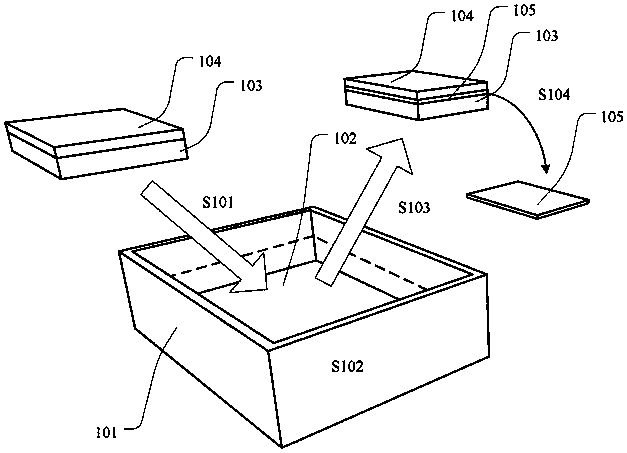
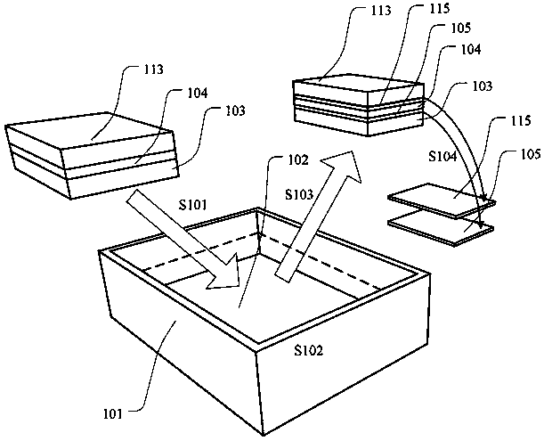
[0035] Hereinafter, the present invention will be described in more detail with reference to the accompanying drawings. In the various figures, identical elements are indicated with similar reference numerals. For the sake of clarity, various parts in the drawings have not been drawn to scale. Also, some well-known parts may not be shown.

[0036] In the following, many specific details of the present invention are described, such as device structures, materials, dimensions, processing techniques and techniques, for a clearer understanding of the present invention. However, the invention may be practiced without these specific details, as will be understood by those skilled in the art.

[0037] The invention can be embodied in various forms, some examples of which are described below.

[0038] In the prior art, monocrystalline bulk materials have been produced by solvothermal method. The solvothermal method is a manufacturing method developed on the basis of the hydrotherm...


PUM


Abstract

The invention discloses a method for producing a superconducting single crystal thin film. The method comprises the following steps: adding an initial laminated structure into a reaction solution in areaction tank, wherein the initial laminated structure includes at least one substrate and a seed crystal layer attached to the at least one substrate; adjusting the temperature of the reaction solution to a predetermined temperature, and keeping the predetermined temperature for a predetermined time to form a product laminated structure, wherein the product laminated structure comprises the at least one substrate, the seed crystal layer and at least one superconducting single crystal thin film; taking out the product laminated structure from the reaction solution, and flushing and drying theproduct laminated structure; and separating the at least one superconducting single crystal thin film from the at least one substrate and the seed crystal layer, wherein the reaction solution includes a solvent and an inorganic precursor, and the inorganic precursor provides active ions for the component of the superconducting single crystal thin film. The method uses the inorganic precursor to provide the active ions and adopts the seed crystal layer as a growth template in order to form the large-size and high-quality superconducting single crystal thin film.

Description

technical field [0001] The invention relates to the field of thin film materials, more specifically, to a method for manufacturing a superconducting single crystal thin film. Background technique [0002] In the practical application and basic research of high-temperature superconducting materials, high-quality superconducting single crystal thin films play an important role. The physical properties of superconducting single crystal thin films are stable, high current density and superconducting transition temperature can be achieved, so they are the basic materials for the development of high-frequency electronic devices and Josephine junction electronic devices. Superconducting single crystal thin films can be produced by physical or chemical methods. Physical methods include magnetron sputtering, electron beam evaporation, molecular beam epitaxy, pulsed laser deposition, etc. Chemical methods include metal organic compound vapor deposition, aerosol deposition, sol gel me...

Claims


Application Information

Patent Timeline
Patent Type & Authority Applications(China)
IPC IPC(8): C30B19/12C30B29/46H01B12/06
CPCC30B19/12C30B29/46H01B12/06Y02E40/60
Inventor 董晓莉赵忠贤袁洁金魁周放黄裕龙冯中沛
Owner INST OF PHYSICS - CHINESE ACAD OF SCI
Why Eureka
Try Eureka