NAND gate flash memory without junction in rear grid and manufacturing method of flash memory

The technology of a flash memory and its manufacturing method is applied in the field of gate-back non-junction NAND flash memory and its manufacture, which can solve the problems of large memory size, high process difficulty, complex structure, etc., and achieve simple memory structure and high channel current. Ease of control, effect of increasing memory cell density

Active Publication Date: 2018-07-20
ZING SEMICON CORP
View PDF6 Cites 3 Cited by
  • Summary
  • Abstract
  • Description
  • Claims
  • Application Information

AI Technical Summary

Problems solved by technology

[0006] In view of the above-mentioned shortcomings of the prior art, the object of the present invention is to provide a gate-back junction-free NAND flash memory and its manufacturing method, which is used to solve the problem of large volume and complex structure of the NAND flash memory in the prior art. , the problem of high technical difficulty

Method used


Image

  • NAND gate flash memory without junction in rear grid and manufacturing method of flash memory
  • NAND gate flash memory without junction in rear grid and manufacturing method of flash memory
  • NAND gate flash memory without junction in rear grid and manufacturing method of flash memory

Examples


Embodiment 1

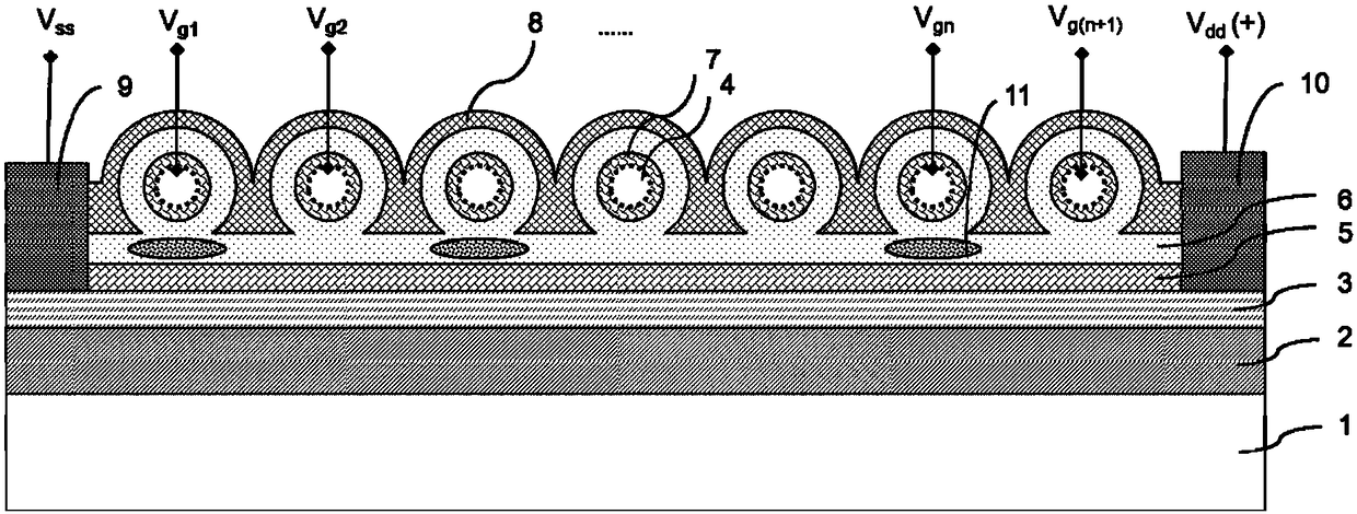
[0063] The present invention provides a gate-last non-junction NAND flash memory, please refer to figure 1 , shown as a schematic diagram of the structure of the memory, including:

[0064] substrate1;

[0065] an insulating layer 2 located on the substrate 1;

[0066] The channel layer 3 is located on the insulating layer 2 and adopts a two-dimensional semiconductor material;

[0067] A grid array of carbon nanotubes, suspended above the channel layer 3, including a number of discrete carbon nanotubes 4, the carbon nanotubes 4 are used as gate electrodes of transistors in the memory;

[0068] The gate trapping structure includes a tunnel layer 5, a charge trapping layer 6, and a blocking layer 7; wherein, the tunneling layer 5 is located on the channel layer 3, and the blocking layer 7 surrounds the outer surface of the carbon nanotube 4, The charge trapping layer 6 includes a first portion surrounding the outer surface of the blocking layer 7 and a second portion located ...

Embodiment 2

[0081] The present invention also provides a method for fabricating a gate-back non-junction NAND flash memory, comprising the following steps:

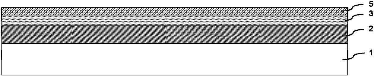
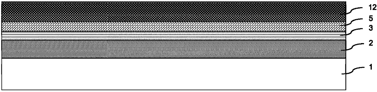
[0082] See first figure 2 A substrate 1 is provided, and an insulating layer 2 , a two-dimensional semiconductor material channel layer 3 and a tunnel layer 4 are sequentially formed on the substrate 1 from bottom to top.

[0083] Specifically, the substrate 1 includes, but is not limited to, a suitable semiconductor substrate such as silicon, germanium, and silicon germanium, and the insulating layer 2 includes, but not limited to, a suitable insulating material such as silicon oxide. For example, the insulating layer may be formed by growing an oxide layer on a silicon substrate.

[0084] The channel layer 3 is made of two-dimensional semiconductor material with a thickness of 1-10 atomic layers. As an example, the two-dimensional semiconductor material is selected from MoS 2 、WS 2 、ReS 2 And any one of SnO, in this embodimen...


PUM


Abstract

The invention provides an NAND gate flash memory without a junction in a rear grid and a manufacturing method of the flash memory. The memory comprises a substrate, an insulating layer, a 2D semiconductor material channel layer, a carbon nanotube grid array, a grid trap structure, a protective layer, a source contact electrode and a drain contact electrode; the grid trap structure comprises a tunnel layer, a charge trap layer and a barrier layer, the tunnel layer is positioned on the channel layer, the barrier layer surrounds outer side surfaces of carbon nanotubes in the carbon nanotube gridarray, and the charge trap layer comprises a first part surrounding the outer side of the barrier layer and a second part positioned on the tunnel layer and making contact with the first part. The NAND gate flash memory without junction in the rear grid uses a horizontal channel of a 2D semiconductor material, the metallic carbon nanotube grid array is used, the barrier layer and the charge trap layer surround the carbon nanotube grid, the device structure is simplified, the density of storage units is improved, and a higher grid charge trap performance can be obtained.

Description

technical field [0001] The invention belongs to the technical field of integrated circuits, and relates to a gate-back non-junction NAND flash memory and a manufacturing method thereof. Background technique [0002] NAND memories with different architectures can be divided into three-dimensional floating gate memories and three-dimensional charge trap memories according to the material division of storage layers. The former is mainly promoted by Micron Corporation of the United States, and the technical preparations were completed at the end of 2015. Since the polysilicon floating gate is used as the storage layer, the area of ​​the storage unit is larger, and the process is more difficult when more layers of storage units are stacked. Therefore, it is mainly Area reduction is achieved by placing peripheral circuitry beneath the memory array. For the latter three-dimensional charge trap memory, it can be divided into vertical gate type and vertical channel type. The three-...

Claims


Application Information

Patent Timeline
Patent Type & Authority Applications(China)
IPC IPC(8): H01L27/1157H01L29/49
CPCH01L29/49H10B43/35
Inventor 肖德元
Owner ZING SEMICON CORP
Why Eureka
Try Eureka