Low-pressure diffusion process applied to polycrystalline black silicon solar cells

A solar cell and diffusion process technology, applied in circuits, photovoltaic power generation, electrical components, etc., can solve problems such as poor sheet resistance uniformity, and achieve the effects of increasing filling factor, increasing surface doping concentration, and improving uniformity

Active Publication Date: 2018-07-24
WUXI SUNTECH POWER CO LTD
View PDF6 Cites 12 Cited by
  • Summary
  • Abstract
  • Description
  • Claims
  • Application Information

AI Technical Summary

Problems solved by technology

Due to the existence of black silicon nano-textured microstructure, the uniformity of sheet resistance after diffusion becomes worse

Method used


Image

  • Low-pressure diffusion process applied to polycrystalline black silicon solar cells
  • Low-pressure diffusion process applied to polycrystalline black silicon solar cells
  • Low-pressure diffusion process applied to polycrystalline black silicon solar cells

Examples


Embodiment 1

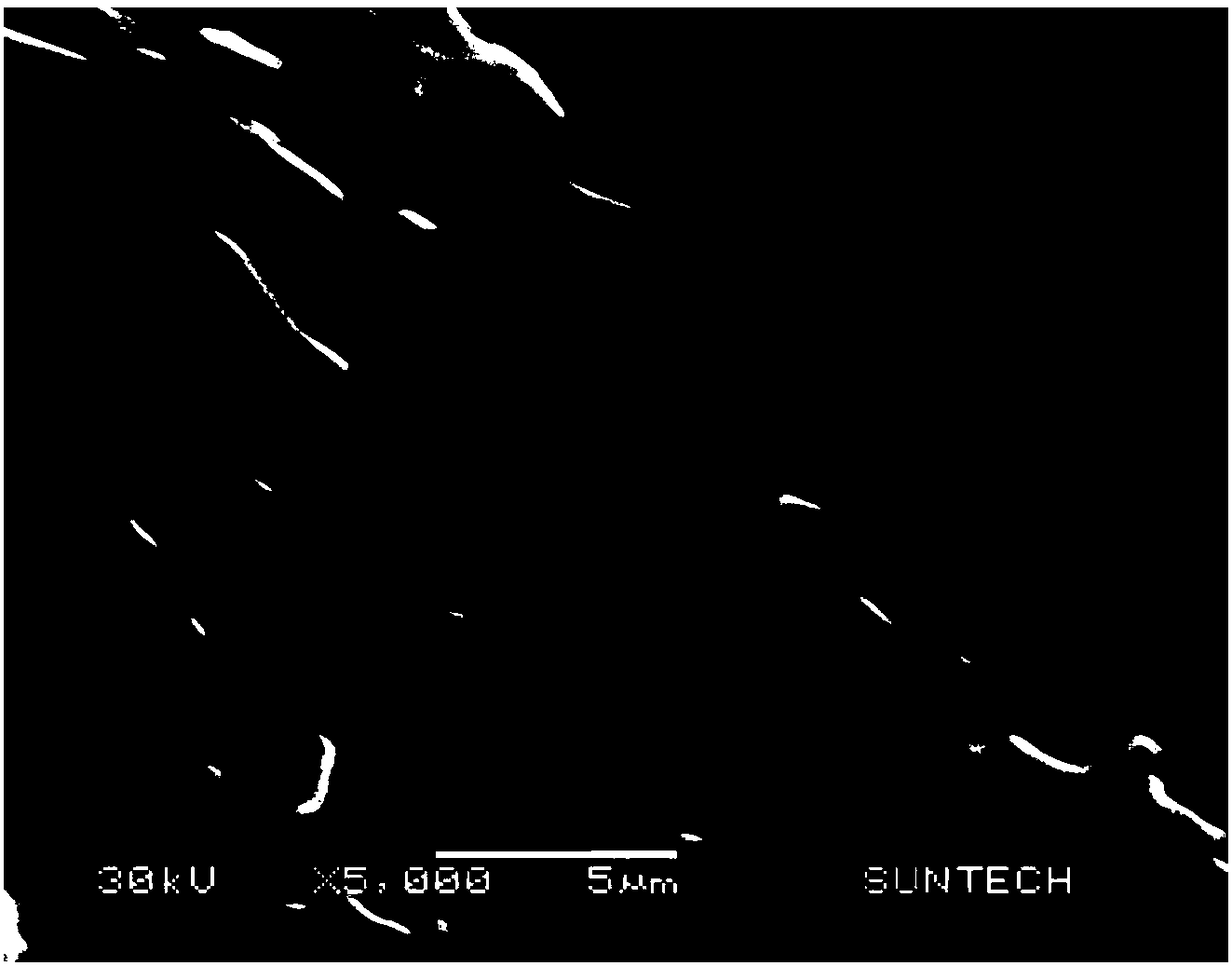
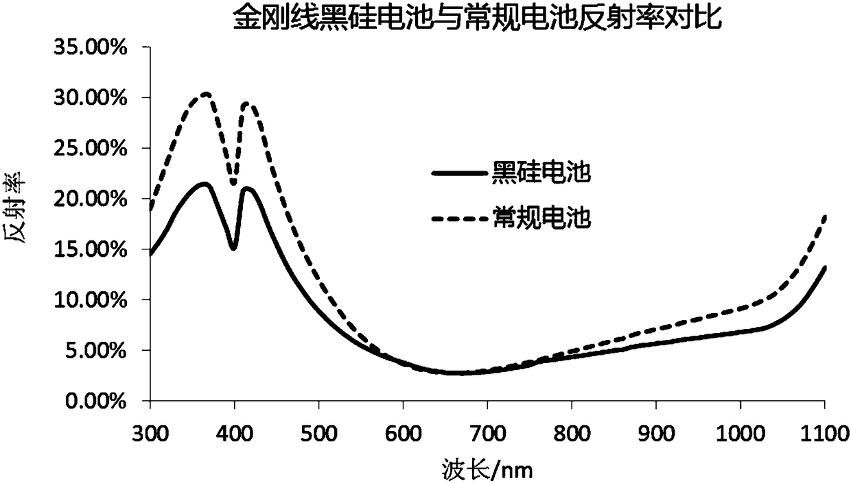
[0029] Choose 156.75mm*156.75mm P-type diamond wire-cut polysilicon wafer as the base material, with a resistivity of 3Ω·cm, after alkali polishing, pickling, immersion silver, digging, desilvering, hole expansion, alkali cleaning, pickling, water washing 1. drying to prepare the textured surface, the thinning amount of the textured surface is 0.38g, the aperture of the nano-textured surface is 500nm, and the surface reflectance of the silicon wafer after the textured process is 19.5%. Load the textured black silicon wafer into the diffusion quartz boat to prepare for diffusion.

[0030] The diffusion process is shown in Table 1:

[0031] Table 1

[0032]

[0033] The sheet resistance value after diffusion according to the process parameters of Example 1. Take 2 slices from the furnace mouth, the middle of the furnace, and the end of the furnace respectively, test the square resistance value of 9 points on each slice, and calculate the average value of the square resistan...

Embodiment 2

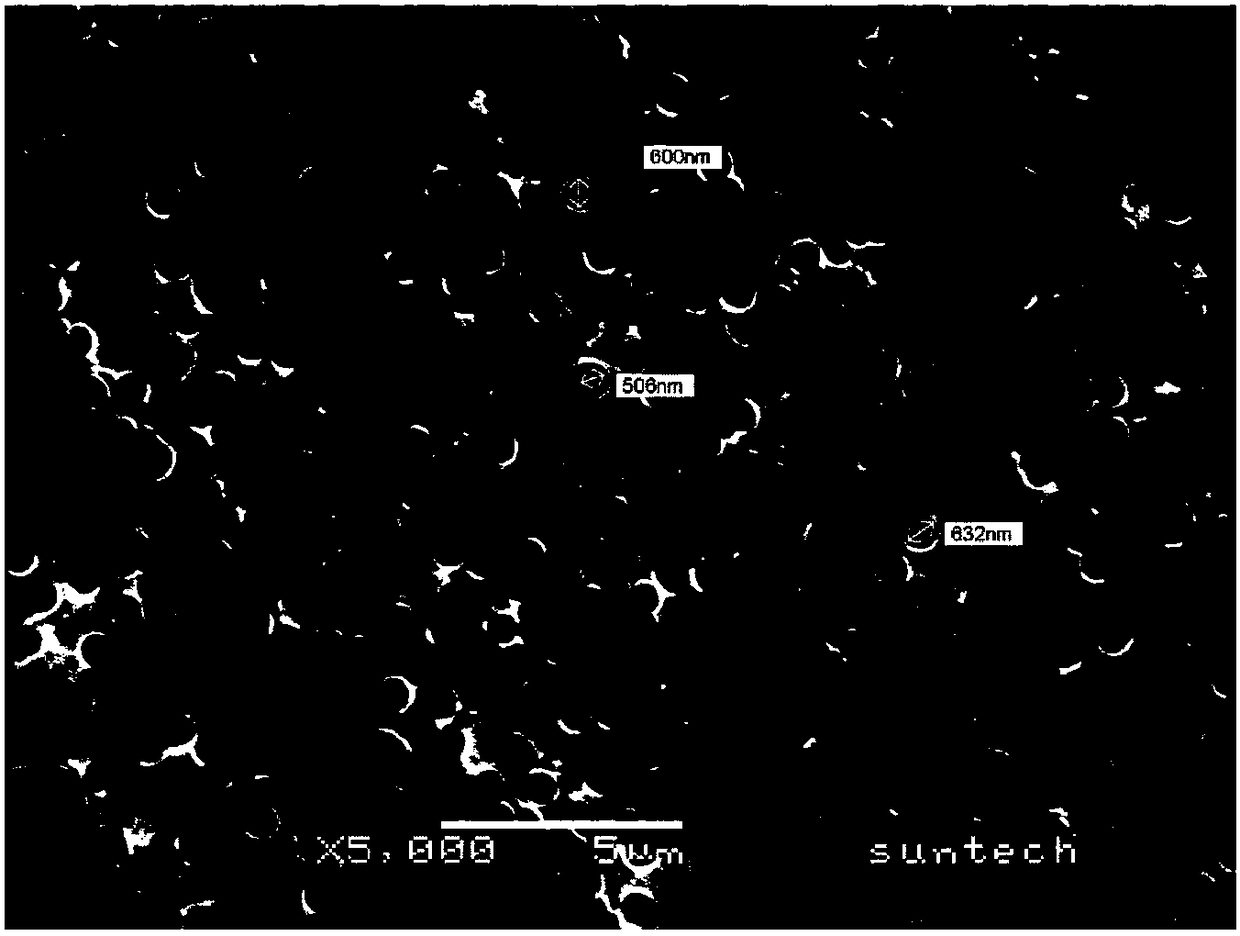
[0043] Choose 156.75mm*156.75mm P-type diamond wire-cut polycrystalline silicon wafer as the base material, with a resistivity of 2Ω·cm, after alkali polishing, pickling, immersion silver, digging, desilvering, hole expansion, alkali cleaning, pickling, water washing 1. drying to prepare the textured surface, the thinning amount of the textured surface is 0.45g, the aperture of the nano-textured surface is 700nm, and the surface reflectance of the silicon wafer after the textured process is 21.0%. The textured black silicon wafers are loaded into the diffusion quartz boat for diffusion.

[0044] The diffusion process is shown in Table 4.

[0045] Table 4

[0046]

[0047]

[0048] Sheet resistance value after diffusion according to the process parameters of Example 2. Take 2 slices from the furnace mouth, the middle of the furnace, and the end of the furnace respectively, test the square resistance value of 9 points on each slice, and calculate the average value of the...


PUM


Abstract

The invention relates to a low-pressure diffusion process applied to polycrystalline black silicon solar cells, which comprises the following steps: (1) allowing a silicon wafer to entering a tube; (2) performing constant temperature processing; (3) performing low temperature oxidation, generating a thin oxide layer on a surface of the silicon wafer to make the subsequent phosphorus source deposition more uniform; (4) performing low temperature deposition, uniformly depositing a phosphorus source on the surface of the silicon wafer; (5) performing high temperature propulsion, allowing the phosphorus source to diffuse into the silicon wafer, wherein during high temperature propulsion, the temperature is 820-850 DEG C, the nitrogen flow rate is 1000-3000sccm, the dry oxygen is 0-1000sccm, the furnace pressure is 50-150mbar, and the time is 10-20 minutes; (6) performing secondary diffusion, wherein during the secondary diffusion, the temperature is 800-850 DEG C, the nitrogen flow rate is1000-3000sccm, the source nitrogen is 0-400sccm, the dry oxygen is 0-1000sccm, the furnace pressure is 50-150mbar, the time is 2-10 minutes; (7) performing cooling; (8) performing nitrogen filling, allowing the pressure inside the pipe to reach the atmospheric pressure so that a furnace door is opened; and (9) performing discharging. The present invention improves the uniformity of the square resistance after diffusion of polycrystalline black silicon.

Description

technical field [0001] The invention relates to a low-voltage diffusion process applied to polycrystalline black silicon solar cells, which belongs to the field of photoelectric technology. Background technique [0002] Reducing costs and improving conversion efficiency of solar cells are the key to the photovoltaic industry gradually replacing traditional energy sources. At present, photovoltaic power generation products on the market are still dominated by polycrystalline solar cell components. Reducing the cost of polycrystalline solar cells and improving the conversion efficiency of polycrystalline solar cells are the key to cost reduction. Polycrystalline silicon wafers are divided into mortar cut silicon wafers and diamond wire cut silicon wafers. Among them, polycrystalline diamond wire-cut silicon wafers have the advantages of fast cutting speed, smaller wire loss compared with mortar cutting, thinner damaged layer, more environmental protection, and low cost. The m...

Claims


Application Information

Patent Timeline
Patent Type & Authority Applications(China)
IPC IPC(8): H01L31/18H01L21/225H01L31/068
CPCH01L21/2252H01L31/068H01L31/1804Y02E10/546Y02E10/547Y02P70/50
Inventor 陈丽萍
Owner WUXI SUNTECH POWER CO LTD
Why Eureka
Try Eureka