Switched capacitor amplifier capable of offset compensation and finite gain compensation

A finite gain, switched capacitor technology, used in amplifiers using switched capacitors, amplifiers with semiconductor devices/discharge tubes, DC-coupled DC amplifiers, etc., can solve problems such as output offset voltage, gain error, DC gain error, etc. , to eliminate charge injection and clock feedthrough, reduce charge transfer errors, and reduce DC offset voltage

Pending Publication Date: 2018-07-24
SHENZHEN INSTITUTE OF INFORMATION TECHNOLOGY
View PDF1 Cites 5 Cited by
  • Summary
  • Abstract
  • Description
  • Claims
  • Application Information

AI Technical Summary

Problems solved by technology

The amplifier compensates the offset voltage by compensating capacitive coupling, but due to the limited gain of the op amp, node A will leave a small signal related to the input signal -V OUT /A, resulting in an input capacitance C 1 charge on the cannot be fully transferred to the output capacitor C 3 Therefore, the output offset voltage can only be reduced to (1+C 1 /C 3 )/A times, and the DC gain error of the amplifier is (1+C 1 /C 3 )/A 2 , where A is the gain of the op amp
If it is necessary to further reduce the offset voltage and gain error of

Method used


Image

  • Switched capacitor amplifier capable of offset compensation and finite gain compensation
  • Switched capacitor amplifier capable of offset compensation and finite gain compensation
  • Switched capacitor amplifier capable of offset compensation and finite gain compensation

Examples


Embodiment Construction

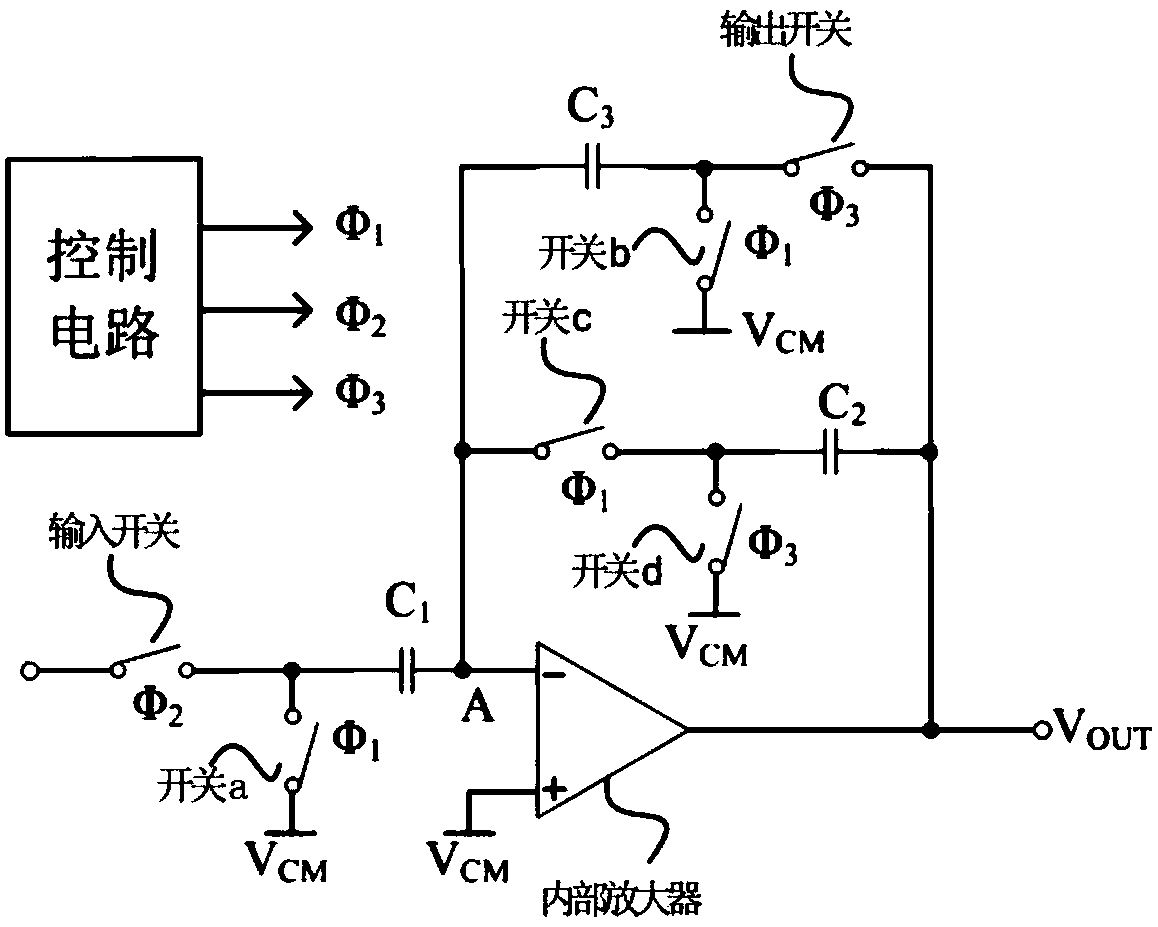
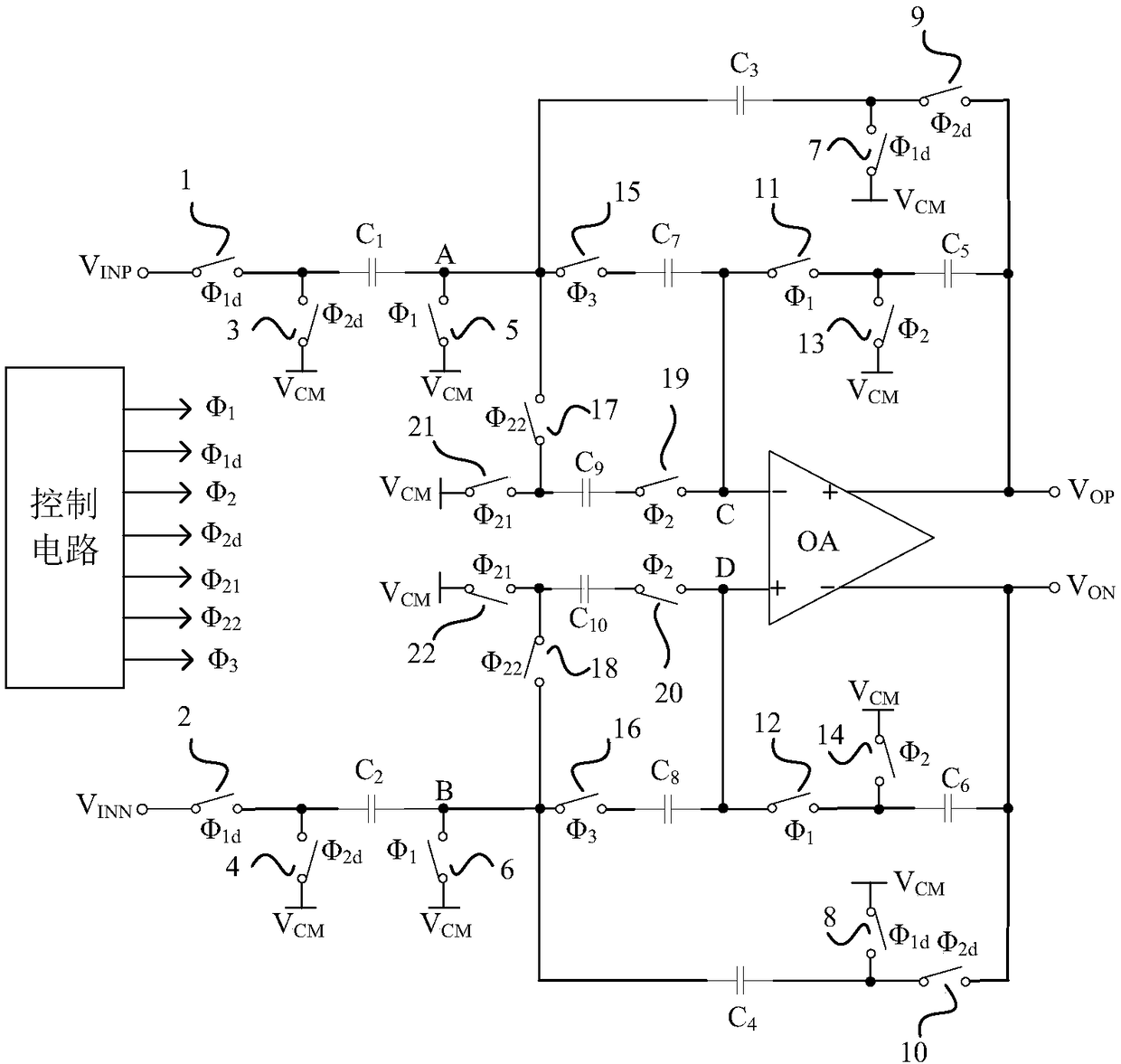
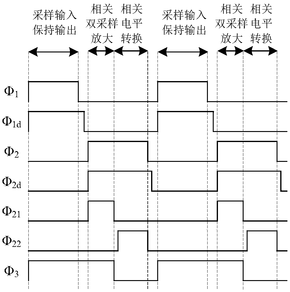
[0033] The specific implementation process of the present invention will be described in detail below in conjunction with the accompanying drawings and specific embodiments. In this embodiment, correlated double sampling and input-correlated level conversion techniques are used to reduce the residual charge on the input capacitor, reduce the DC offset voltage of the switched capacitor amplifier, and improve the gain accuracy of the amplifier.

[0034] First, explain the structure of the switched capacitor amplifier, figure 2 Is given is the circuit diagram of the switched capacitor amplifier proposed by the present invention. The switched capacitor amplifier includes a related double-sampling finite gain compensation branch, an offset voltage storage branch, a related level conversion branch, a fully differential operational amplifier OA and a control circuit. The correlated double-sampled finite-gain compensation branch includes an input capacitor C 1 、C 2 , the output ca...


PUM


Abstract

The invention discloses a switched capacitor amplifier capable of offset compensation and finite gain compensation. The switched capacitor amplifier comprises a correlated double sampling finite gaincompensation branch, an offset voltage storage branch, a correlated level switch branch, a fully-differential operation OA, and a control circuit. The switched capacitor amplifier provided by the invention has the advantages that through the correlated double sampling technology and the input correlated level switch technology, charges remained on an input capacitor and charge transfer errors caused by finite gains of operation are reduced, so that an output DC offset voltage is reduced and higher gain precision of the amplifier is achieved; and the switched capacitor amplifier adopts a fully-differential structure to eliminate charge injection and clock feedthrough, and achieves a small DC offset voltage, high gain precision, etc.

Description

technical field [0001] The invention relates to the field of high-precision analog circuit design, in particular to a switched capacitor amplifier for offset compensation and finite gain compensation. Background technique [0002] Switched capacitor amplifiers are widely used in various low-power and high-precision analog circuits, such as instrumentation amplifiers for smart sensor systems, and sense amplifiers for biomedical signal acquisition systems. The signals processed by these amplifiers have low frequency and small signal amplitude, and usually require the output DC offset voltage of the amplifier to be small and the gain error to be small. The performance of the switched capacitor amplifier is affected by many nonlinear factors, such as the offset voltage of the op amp, finite gain, switch charge injection, clock feedthrough, thermal noise of the circuit, etc., which will affect the output DC offset voltage and output gain of the amplifier. Among many factors, the...

Claims


Application Information

Patent Timeline
IPC IPC(8): H03F1/30H03F3/00H03F3/45
CPCH03F1/303H03F3/005H03F3/45475
Inventor 陈艳郭艳
Owner SHENZHEN INSTITUTE OF INFORMATION TECHNOLOGY
Why Eureka
Try Eureka