Preparation method of printed circuit board and copper foil for processing

A printed circuit board and copper foil technology, which is applied in the fields of printed circuit manufacturing, printed circuit, printed circuit parts, etc., can solve the problems of endangering the health of the staff, the health of the operator, and the inability to reuse, so as to reduce the production time , avoid the infringement of toxic substances, and reduce the effect of labor costs

Active Publication Date: 2018-07-24
北京启创驿讯科技有限公司
View PDF7 Cites 4 Cited by
  • Summary
  • Abstract
  • Description
  • Claims
  • Application Information

AI Technical Summary

Problems solved by technology

[0005] ① Corrosion in corrosive liquids is very dangerous, and it is easy to cause harm to the body of the operator and endanger the health of the staff
[0006] ②The corroded copper foil is lost in the corrosion solution and cannot be reused, resulting in waste of raw materials
[0007] ③ A large amount of chemical waste water is produced, which has high treatment costs and great environmental hazards

Method used


Image

  • Preparation method of printed circuit board and copper foil for processing

Examples


preparation example Construction

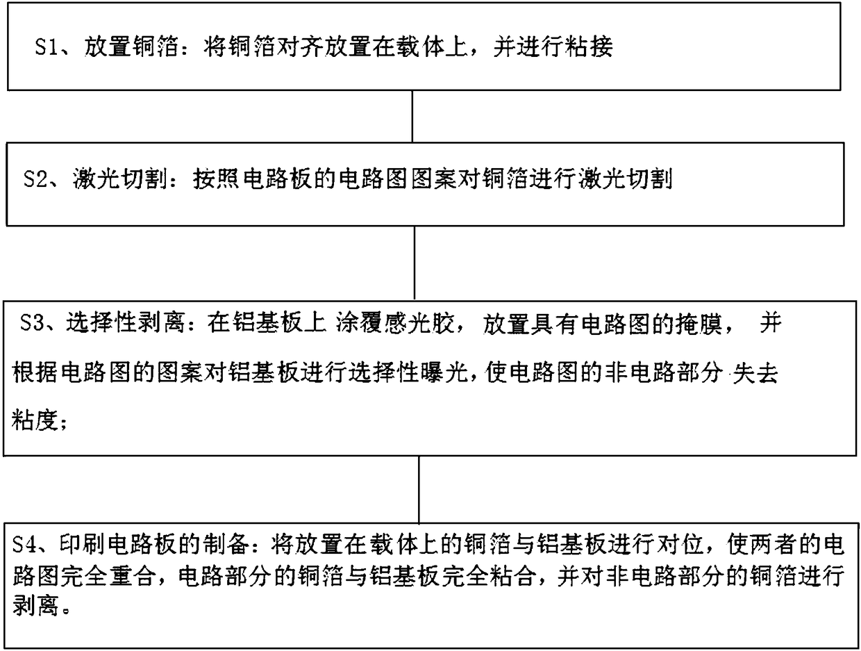
[0033] The invention provides a method for preparing a circuit board, such as figure 1 As shown, it includes the following steps:

[0034] S1. Place the copper foil: place the copper foil on the carrier and compound it with sticky substances;

[0035] S2. Laser cutting: laser cutting the copper foil according to the circuit diagram pattern of the circuit board;

[0036] S3. Selective peeling: Coating photosensitive glue on the aluminum substrate, and placing a mask with a circuit diagram, selectively exposing the aluminum substrate according to the pattern of the circuit diagram, so that the non-circuit part of the circuit diagram loses viscosity;

[0037] S4. Preparation of printed circuit board: Use the alignment device to accurately align the copper foil placed on the carrier with the aluminum substrate, so that the circuit diagrams of the two are completely overlapped, and the copper foil of the circuit part is completely bonded to the aluminum substrate, and the The cop...

specific Embodiment 1

[0046] The working principle of the present invention is further explained below in conjunction with specific embodiments:

[0047] 1. Preparation of photosensitive adhesive

[0048] Mix epoxy resin, calcium hydrogen carbonate, silicone resin, epoxy acrylic photosensitive resin, magnesium hydroxide, aluminum hydroxide, and diluent in a ratio of 50:2:0.03:60:1:10:20:20:80 After stirring and dissolving evenly, use sand mill equipment to grind to a fineness of less than 5 microns; add dihydroamine curing agent and imidazole catalyst, measure the viscosity and pack it after the viscosity is qualified.

[0049] 2. Laser cutting to obtain circuit boards

[0050] Align and place the copper foil on the carrier and bond it; in S1, the copper foil is placed on the PET substrate through an adhesive substance. Laser cut the copper foil according to the circuit diagram pattern of the circuit board; apply photosensitive glue on the aluminum substrate, place a mask with a circuit diagram, ...


PUM


Abstract

The invention provides a preparation method of a printed circuit board. The method includes the following steps of: S1, copper foil arrangement: copper foil is arranged on a carrier in a manner that the copper foil is aligned with the carrier, and the copper foil and the carrier are composited; S2, laser cutting: laser cutting is performed on the pattern of the circuit diagram of a circuit board;S3, selective peeling: an aluminum substrate is coated with photoresist, and a mask with a circuit diagram is arranged on the aluminum substrate, and the aluminum substrate is selectively exposed according to the pattern of the circuit diagram, so that the non-circuit portion of the circuit diagram loses viscosity; and S4, printed circuit board preparation: the copper foil arranged on the carrieris aligned with the aluminum substrate, so that the circuit diagrams of the copper foil and the aluminum substrate are completely overlapped with each other, and the copper foil of a circuit portion is completely bonded to the aluminum substrate, and the copper foil of a non-circuit portion is peeled off. According to the preparation method of the invention, the circuit board is inscribed by a laser cutting method, so that chemical etching can be avoided in a production process; and waste copper can be directly recycled, and therefore, a great environmental protection value can be realized with cost reduced. With the method adopted, a new idea is provided for the production of copper foil for circuit board.

Description

technical field [0001] The invention relates to a method for preparing a printed circuit board, in particular to a method for preparing a printed circuit board and copper foil for processing. Background technique [0002] The layout of the printed circuit board needs to use copper foil to describe the circuit. Therefore, copper foil is widely used in the field of printed circuit board applications. , but now the mainstream is still the subtraction method, in which copper foil is used and excess parts are removed by etching to form circuits on circuit boards. [0003] For example, the invention patent with application number 2014103931912 provides a circuit board and its manufacturing method, and removes excess copper foil by uniformly etching away the copper foil layer in the etched area. [0004] The current etching method is mainly to place the copper foil on the substrate, coat and corrode the coating on the part where the circuit board needs to be described, and then pl...

Claims


Application Information

Patent Timeline
Patent Type & Authority Applications(China)
IPC IPC(8): H05K3/20H05K1/09G03F7/039G03F7/004
CPCG03F7/004G03F7/039H05K1/09H05K3/20H05K2203/107
Inventor 曹昕
Owner 北京启创驿讯科技有限公司
Why Eureka
Try Eureka