A kind of optical device and its preparation and application

A technology for optical devices and optical products, which is applied in the field of materials and can solve problems such as expensive equipment and complex

Active Publication Date: 2020-06-12
NINGBO INST OF MATERIALS TECH & ENG CHINESE ACADEMY OF SCI
View PDF3 Cites 0 Cited by
  • Summary
  • Abstract
  • Description
  • Claims
  • Application Information

AI Technical Summary

Problems solved by technology

The film-forming process of such inorganic or metallic materials often requires complex and expensive equipment

Method used


Image

  • A kind of optical device and its preparation and application
  • A kind of optical device and its preparation and application
  • A kind of optical device and its preparation and application

Examples


preparation example Construction

[0092] The present invention also provides a method for preparing the optical device, comprising the following steps:

[0093] 1) Provide the first mixed liquid, substrate and monomer A, wherein,

[0094] The first mixed solution includes monomer B, an acid-binding agent and a first solvent, and the monomer B is hexachlorocyclotriphosphazene;

[0095] The monomer A is a compound containing n functional groups selected from the following group: hydroxyl, amino, or a combination thereof, where n is 2-10;

[0096] 2) placing the substrate in the first mixed solution, and carrying out the first-stage reaction at the first temperature under agitation;

[0097] 3) Adding the monomer A to the product obtained in the previous step, continuing the second-stage reaction at a second temperature under agitation, and taking out the treated substrate to obtain the optical device.

[0098] In another preferred example, after step 3), the following steps are also included:

[0099] 4) Soxh...

Embodiment 1

[0148] Embodiment 1 Optical device 1 (using silicon wafer as substrate)

[0149] Dissolve 3ml of triethylamine and 0.2g of hexachlorocyclotriphosphazene in 50ml of anhydrous acetonitrile, add a 12×70mm single-polished silicon wafer (0.5mm in thickness) to the above solution, and stir the reaction at 40°C After 1 hour, add 0.8g of 4,4'-diaminodiphenyl ether into the above solution, continue to stir and react at 40°C for 5 hours, take out the silicon chip, and clean it by Soxhlet extraction Dry in a vacuum oven for 0.5 hour to obtain a silicon wafer on which a ring-based cross-linked polyphosphazene film 1 is deposited on the surface, that is, an optical device 1 .

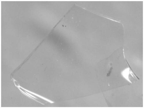
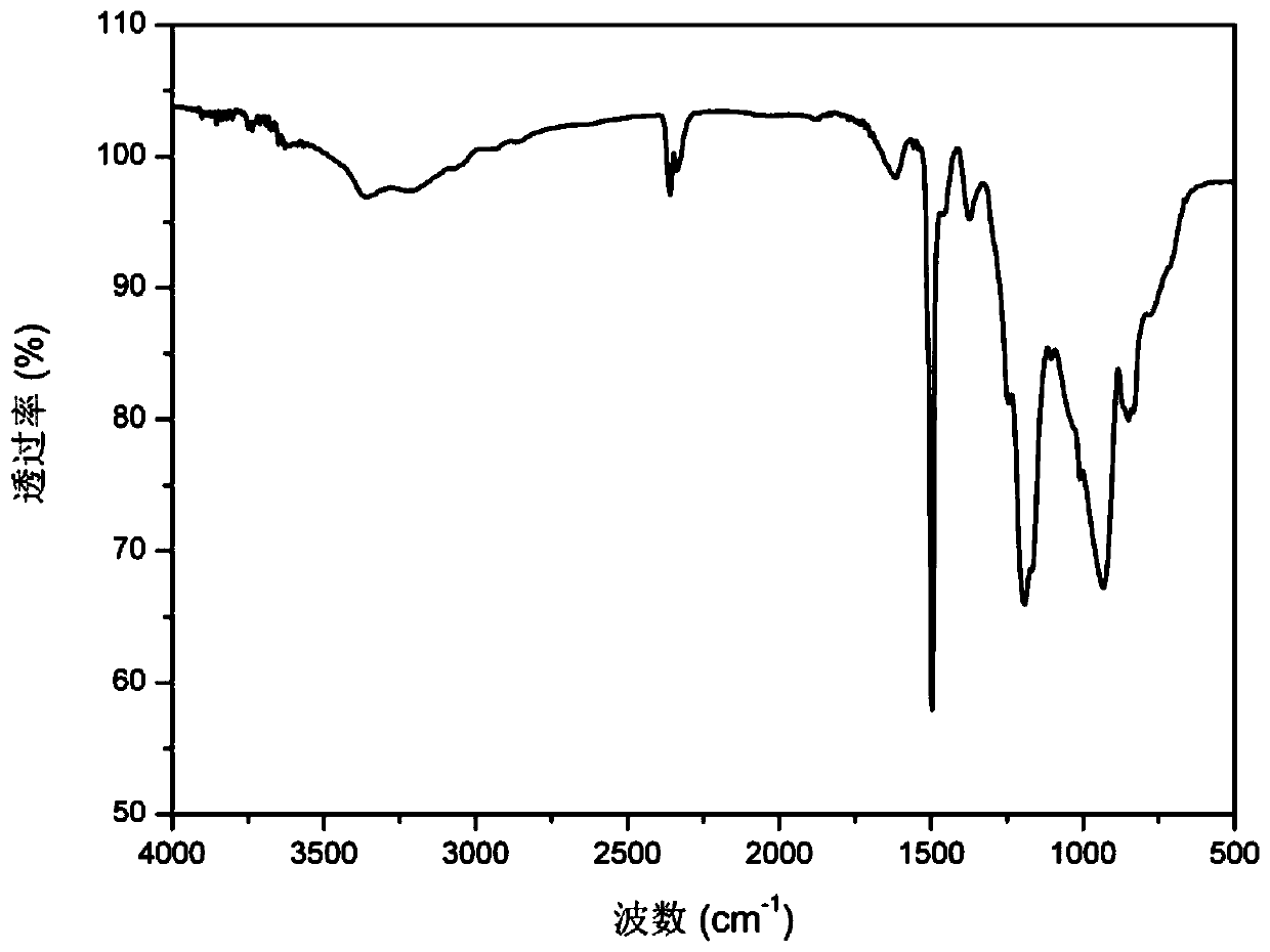
[0150] figure 1 It is an optical microscope photo of the ring-based cross-linked polyphosphazene film 1 peeled off from the silicon wafer. It can be seen that the film has good transparency. After testing, the light transmittance of the film 1 to visible light is ≥ 95%.

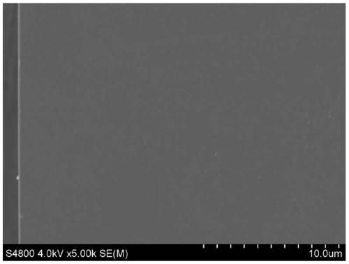
[0151] After further testing, the thicknes...

Embodiment 2

[0157] Example 2 Optics 2

[0158] With embodiment 1, difference is: prolong reaction time to 6 hours.

[0159] The performance of the polyphosphazene film 2 in the optical device 2 is basically the same as that of the polyphosphazene film 1 in the optical device 1, and the thickness of the polyphosphazene film 2 is 735nm.

[0160] Further tests show that the optical device 2 has excellent light selection and regulation performance, and the polyphosphazene film 2 of the optical device 2 can reflect orange-red light, and the reflectance measured by a reflectance spectrometer can reach 66%.


PUM

PropertyMeasurementUnit
surface roughnessaaaaaaaaaa
thicknessaaaaaaaaaa
wavelengthaaaaaaaaaa

Abstract

The invention relates to an optical device and preparation and application thereof. In particular, the invention discloses an optical device comprising a substrate and a polyphosphazene film that is recombined on at least one main surface of the substrate and has the film interference property. In addition, the invention also discloses preparation and application of the optical device. The opticalfilm has advantages of simple preparation method, low cost, stable film structure, and the like; the polyphosphazene film has an excellent film interference effect; and the optical device having thesingle polyphosphazene film has high light selectivity and light regulation.

Description

technical field [0001] The invention relates to the field of materials, in particular to an optical device and its preparation and application. Background technique [0002] Optical thin films are an important part of optical devices and play an irreplaceable role. The common ones are anti-reflection coating, anti-reflection coating and so on. For example, coating a layer of anti-reflection coating on the surface of the lens or lens can reduce the intensity of reflected light and increase the intensity of transmitted light, making the imaging of the optical system clearer. The main working principle of the optical film is: the light has film interference on the surface of the optical film, and the wavelength and intensity of the incident light and the reflected light are screened and adjusted. Common materials that can be used as optical films are mainly some transparent inorganic materials or metal materials, such as magnesium fluoride (MgF 2 ), silicon dioxide (SiO 2 )...

Claims


Application Information

Patent Timeline
Patent Type & Authority Patents(China)
IPC IPC(8): G02B1/10G02B1/11
CPCG02B1/10G02B1/111
Inventor 徐海兵郭彦丽陈祥颜春刘东祝颖丹
Owner NINGBO INST OF MATERIALS TECH & ENG CHINESE ACADEMY OF SCI
Why Eureka
Try Eureka