

Groove infield plate buried layer termination structure of semiconductor device and manufacturing method
A terminal structure, semiconductor technology, applied in semiconductor/solid-state device manufacturing, semiconductor devices, electric solid-state devices, etc., can solve the problems of destroying the wafer, the optimization degree of terminal voltage efficiency and terminal area is difficult to achieve great improvement, etc. The effect of high terminal efficiency
- Summary
- Abstract
- Description
- Claims
- Application Information
AI Technical Summary
Problems solved by technology
Method used
Image

Examples
preparation example Construction
[0050] The preparation method includes: providing a semiconductor substrate, the semiconductor substrate has a plurality of grooves and a plurality of semiconductor pillars, and two adjacent grooves are separated by semiconductor pillars. Push-junction is performed from one or more of the plurality of semiconductor pillars to the body of the semiconductor substrate to form a floating buried doping layer extending below the bottom of the trench. Inner field plates are formed in some of the plurality of trenches. Wherein, the part of the floating doping diffusion buried layer below the bottom of the trench is partially connected, or completely connected, or partially spaced, or completely spaced.
[0051] Further, as a preferred solution, the preparation method includes:
[0052] forming a selective implant mask on the surface of the semiconductor substrate;
[0053] Perform impurity implantation with a conductivity type opposite to that of the semiconductor substrate to form ...
Embodiment 1
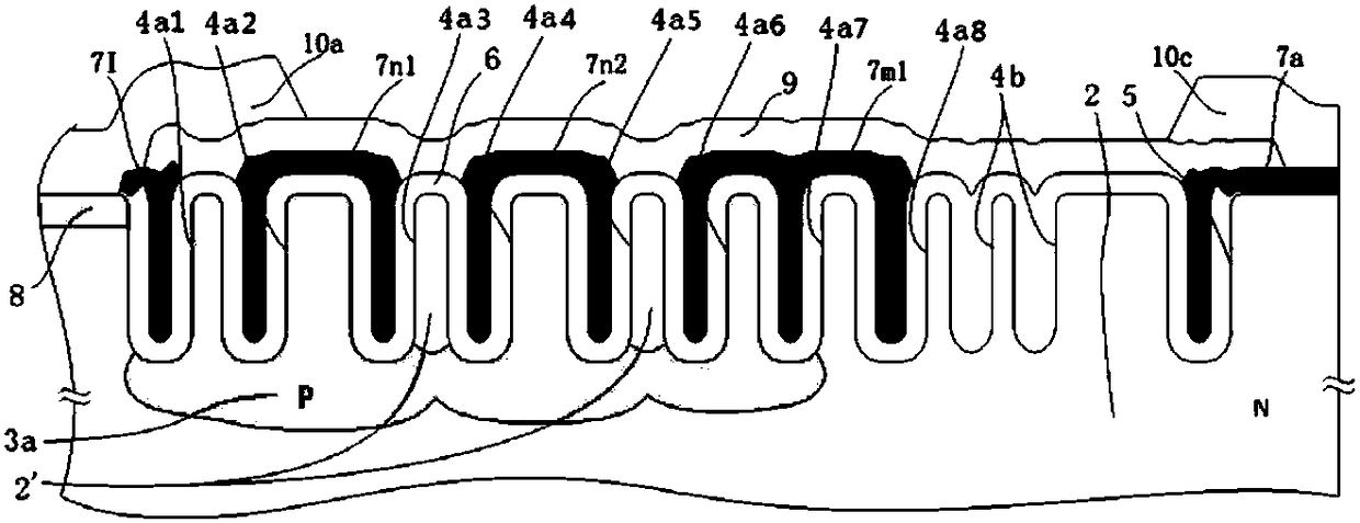
[0063] see figure 1 , this embodiment provides a terminal structure of a semiconductor device.
[0064] like figure 1 As shown, the terminal portion of the semiconductor device is a patterned structure formed on the N-type semiconductor 2 .
[0065] The terminal part includes a plurality of grooves with regular density. The figure shows groove 4a1 , groove 4a2 , groove 4a3 , groove 4a4 , groove 4a5 , groove 4a6 , groove 4a6 , groove 4a8 , groove 4b and groove 5 .
[0066] In the plurality of trenches, each trench has a field oxide layer 6 , and all the field oxide layers 6 extend from the trench to the top surface of the terminal structure and are further connected as a whole. Additionally, if figure 1 As shown, the field oxide layer 6 is completely filled in the trench 4b (the oxide filling formed by the field oxidation in the trench 4b). The field oxide layer 6 formed in the trench 4a1, the trench 4a2, the trench 4a3, the trench 4a4, the trench 4a5, the trench 4a6, the ...
Embodiment 2
[0077] refer to Figure 2-Figure 19 , the present invention provides a method for manufacturing the terminal structure of the field plate buried layer in the trench of the semiconductor device described in Embodiment 1.
[0078] The manufacturing method includes the following steps:
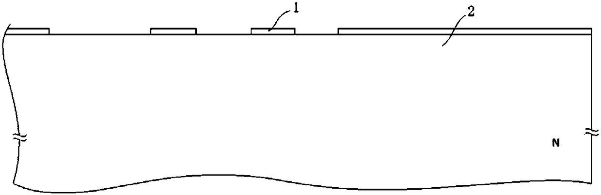
[0079] Step 1: On the surface of N-type semiconductor 2 (single wafer or epitaxial wafer, such as silicon single wafer or silicon epitaxial wafer), form a selective implantation mask 1, such as figure 2 shown.
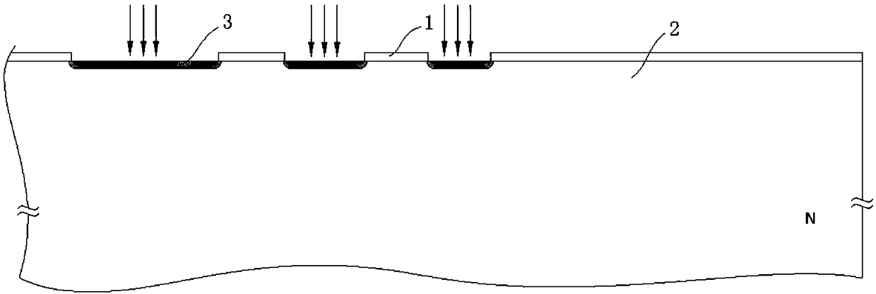
[0080] Step 2: Perform P-type impurity implantation to form a P-type impurity-doped layer 3 (with the opposite conductivity type to the N-type semiconductor 2), such as image 3 shown. After implantation, the selective implantation mask 1 (mask layer) is removed.
[0081] Step 3: Form a trench etching mask 11 after the photolithography process by thermal oxidation or depositing an oxide layer, such as Figure 4 shown.
[0082] Step 4: Perform trench etching.
[0083] The etching d...
PUM
 Abstract
Description
Claims
Application Information