LED substrate transferring method and application thereof

A substrate transfer, LED chip technology, applied in electrical components, circuits, semiconductor devices, etc., can solve the problems of long bonding speed and surface time, metal Sn is easily oxidized, poor bonding effect, etc., and achieves fast bonding speed. , Good eutectic effect and reduced stacking thickness requirements

Inactive Publication Date: 2018-08-03
ENRAYTEK OPTOELECTRONICS
View PDF0 Cites 2 Cited by
  • Summary
  • Abstract
  • Description
  • Claims
  • Application Information

AI Technical Summary

Problems solved by technology

[0006] The purpose of the present invention is to provide a LED substrate transfer method and its application, which solves the influence caused by the prior art due to the thicker bonding layer, long bonding speed surface time, and metal Sn is easily oxidized. The problem of poor bonding effect and low yield can increase the bonding speed and improve the bonding yield

Method used


Image

  • LED substrate transferring method and application thereof
  • LED substrate transferring method and application thereof

Examples


preparation example Construction

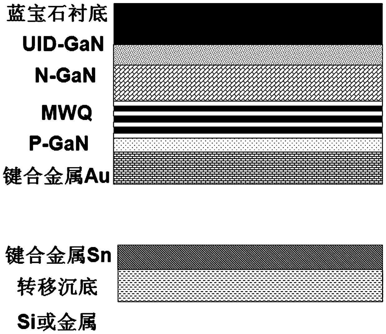
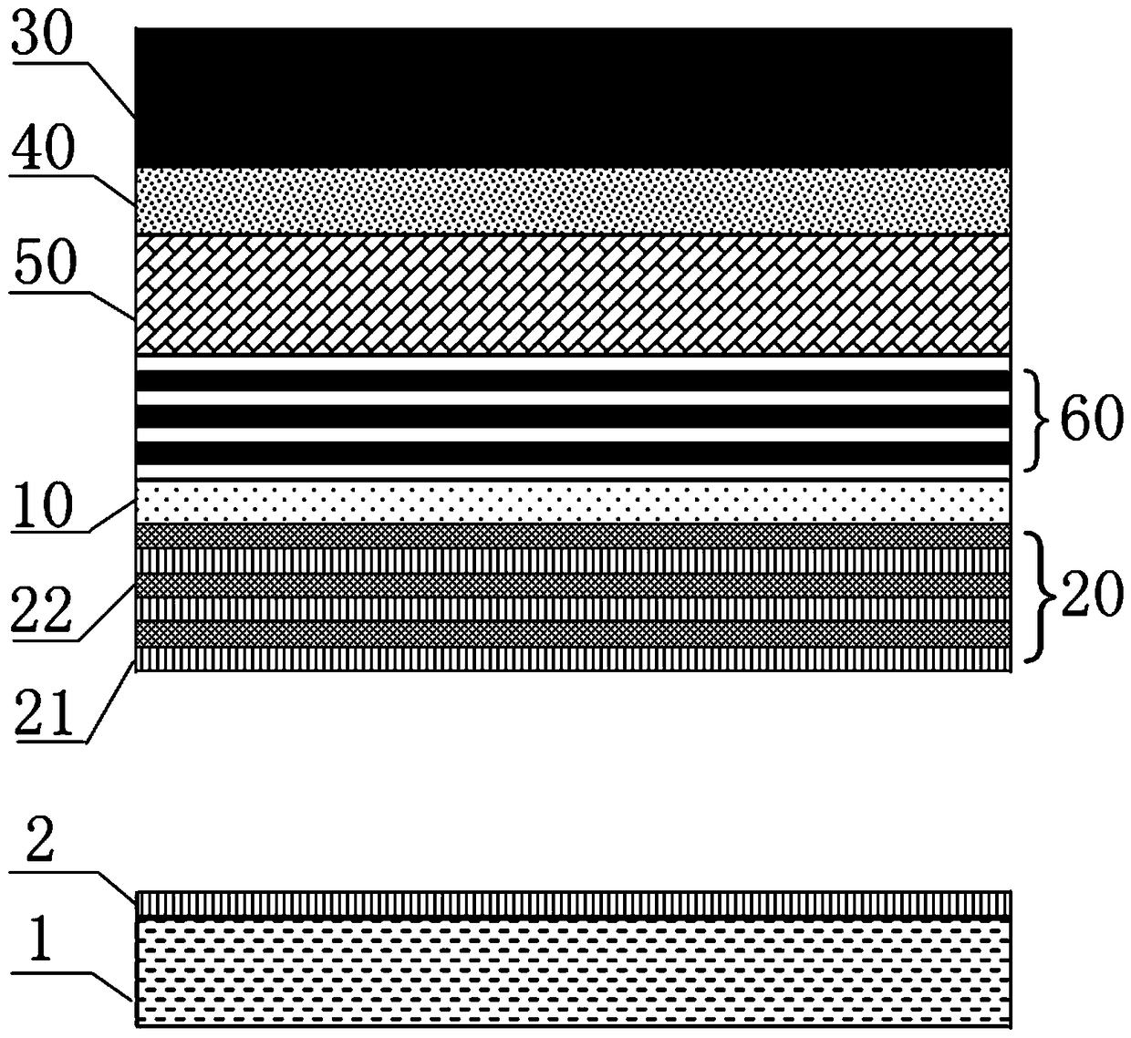
[0035] A method for preparing a vertical LED chip structure, the method comprising: sequentially growing a UID-GaN layer 40, an N-GaN layer 50, a MWQ layer 60, and a P-GaN layer 10 on a sapphire substrate 30; The transfer method carries out the substrate transfer; the sapphire substrate 30 is peeled off; the UID-GaN layer 40 is removed; the GaN located in the scribe area is removed on the surface of the N-GaN layer 50; the surface of the N-GaN layer 50 is roughened; electrode.

[0036] The sapphire substrate 30 is lifted off using a laser lift-off process; the UID-GaN layer 40 is removed using an ICP etching process.

[0037] On the surface of the N-GaN layer 50, the part where the step structure is formed is provided with SiO 2 Mask layer, remove part of GaN located in the scribe area; remove SiO 2 The mask layer is used to remove the GaN remaining in the scribe line region, and at the same time form a stepped structure.

[0038] The roughening of the surface of the N-GaN ...

Embodiment 1

[0041] A method for turning an LED substrate, the method comprising:

[0042] (1) The bonding metal layer 20 is grown on the P surface of the P-GaN layer 10 of the LED structure. The bonding metal layer 20 is grown by stacking several Au layers 21 and Sn layers 22, that is, through an electron gun metal evaporation machine Evaporation, first grow a layer of Au with a thickness of 327nm±5%, then grow a layer of Sn with a thickness of 2970nm±5%, repeat several times, stack at least two pairs of Au / Sn, and finally grow another layer of Au , the molecular mass ratio of each pair of Au / Sn is (80±5):(20±5);

[0043] (2) Grow an adhesive Au layer 2 on the surface of the transfer substrate Si 1, and the thickness of the Au layer 1 is not less than 1000A;

[0044] (3) Metal bonding is performed on the bonding metal layer 20 and the bonding Au layer 2 under the conditions of a pressure of 3000-8000 mBar and a temperature of 270-310° C. for 25-30 minutes to complete the substrate transf...

Embodiment 2

[0047] A method for preparing a vertical LED chip structure, the method comprising:

[0048] (1) On the sapphire substrate 30, grow UID-GaN layer 40, N-GaN layer 50, MWQ (multiple quantum well) layer 60 and P-GaN layer 10 in sequence;

[0049] (2) Using the LED substrate transfer method of Embodiment 1 to transfer the substrate;

[0050] (3) Using a laser lift-off process to lift off the sapphire substrate 30;

[0051] (4) The UID-GaN layer 40 is removed by using an ICP etching process, and the etching gas used in the ICP etching process includes Cl 2 and / or BCl 3 ;

[0052] (5) SiO is provided on the part where the step structure is formed on the surface of the N-GaN layer 50 2 The mask layer, using ICP etching process to remove part of the GaN located in the scribe area;

[0053] (6) Removal of SiO 2 Mask layer, using wet etching process (etching with hot acid solution) to remove GaN remaining in the scribe line area, and simultaneously form a stepped structure;

[00...


PUM

PropertyMeasurementUnit
thicknessaaaaaaaaaa
thicknessaaaaaaaaaa

Abstract

The invention discloses an LED substrate transferring method and an application thereof. The LED substrate transferring method comprises the steps of: growing a bonding metal layer on a P surface of aP-GaN layer of an LED structure, wherein the bonding metal layer is formed by growing a plurality of pairs of Au layers and Sn layers in a stacked manner, and at least two pairs of the Au layers andthe Sn layers are stacked; growing an adhesive Au layer on a Si surface of a transferred substrate; and performing metal bonding on the bonding metal layer and the adhesive Au layer to complete substrate transfer. The LED substrate transferring method solves the problems of poor bonding effect and low yield caused by the conditions that the thickness of the bonding layer is large, the bonding speed surface time is long and the metal Sn is prone to oxidize in the prior art, can accelerate the bonding speed, and increases the bonding yield.

Description

technical field [0001] The invention relates to a substrate transfer method, in particular to an LED substrate transfer method and application thereof. Background technique [0002] Light Emitting Diode (LED, Light Emitting Diode) is a kind of semiconductor diode that converts electrical energy into light energy. The internal structure of the LED is divided into a P region and an N region, and the junction of the P region and the N region forms a PN junction. The PN junction has unidirectional conductivity, which is a characteristic utilized by many devices in electronic technology. [0003] GaN-based vertical structure LED is a hot spot in the research of semiconductor devices. GaN-based vertical structure LED has the advantages of good heat dissipation, high current carrying capacity, high luminous intensity, low power consumption and long life. It is widely used in general lighting, landscape lighting, special lighting, automotive widely used in lighting. [0004] In t...

Claims


Application Information

Patent Timeline
Patent Type & Authority Applications(China)
IPC IPC(8): H01L33/00H01L21/78
CPCH01L21/7813H01L33/0075
Inventor 王亚洲朱酉良
Owner ENRAYTEK OPTOELECTRONICS
Why Eureka
Try Eureka