
Superjunction-based integrated power device and manufacturing method thereof

A technology of integrated power and manufacturing methods, which is applied in the field of power semiconductor devices, can solve the problems of circuit miniaturization, large occupied area, and high integration level, and is beneficial to system integration and miniaturization, low cost, and high reliability. Effect

Active Publication Date: 2021-09-07
UNIV OF ELECTRONICS SCI & TECH OF CHINA
View PDF5 Cites 0 Cited by
  • Summary
  • Abstract
  • Description
  • Claims
  • Application Information

AI Technical Summary

Problems solved by technology

[0003] Power MOS devices are widely used in LED drive power supplies, chargers, power adapters and other products. The integrated circuits used in the existing circuit applications of these products integrate traditional power VDMOS devices by forming an isolation structure between devices. Together, for the sake of process compatibility, most of the isolation is reverse junction isolation composed of deep wells and epitaxial layers. This traditional VDMOS power device and second doping type well isolation has large leakage and occupies an area of Large, high cost, does not meet the requirements of the current development of power electronics technology for circuit miniaturization and high integration

Method used


Image

  • Superjunction-based integrated power device and manufacturing method thereof
  • Superjunction-based integrated power device and manufacturing method thereof
  • Superjunction-based integrated power device and manufacturing method thereof

Examples


Embodiment 1

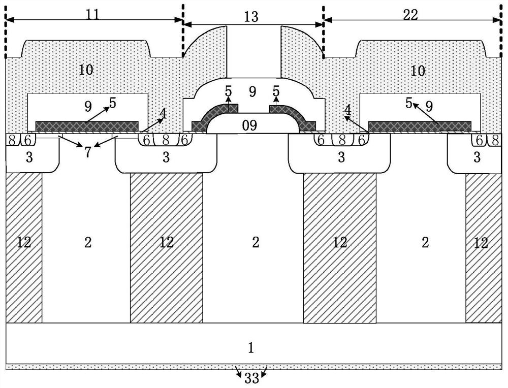
[0048] Such as figure 1 As shown, a superjunction-based integrated power device, its cell structure includes a first doping type substrate 1, and the first doping type substrate 1 is provided with an enhancement superjunction MOSFET 22, a depletion superjunction MOSFET Junction MOSFET11 and an isolation structure 13, two super-junction MOSFET devices share the drain, the isolation structure 13 is arranged between the enhanced super-junction MOSFET22 and the depletion-type super-junction MOSFET11, and the drain metal is arranged under the substrate 33;

[0049] The enhanced super junction MOSFET 22 includes second doping type strips 12 and first doping type strips 2 alternately arranged on the first doping type substrate 1, and the second doping type strips 12 and first doping type strips alternately arranged Above the doping type strip 2 are two second doping type well regions 3; two first doping type heavily doped source regions 6 are respectively arranged in the second dopi...

Embodiment 2

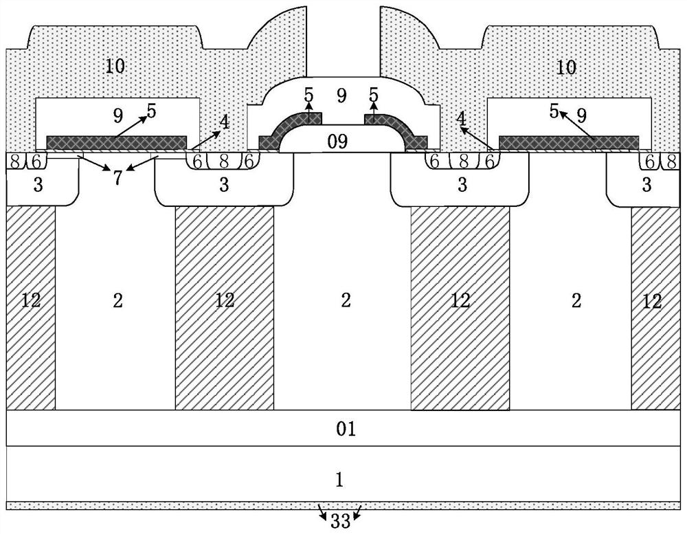
[0076] Such as figure 2As shown, a superjunction-based integrated power device of this embodiment differs from Embodiment 1 in that: the substrate 1 of the first doping type alternates with strips 12 of the second doping type and the first doping type The first doping type doping Buffer layer 01 is arranged between the drift regions formed by the impurity type strips 2 .

Embodiment 3

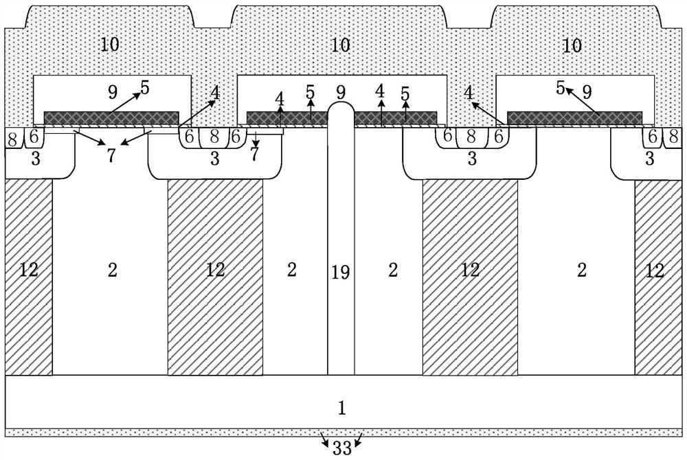
[0078] Such as image 3 As shown, a superjunction-based integrated power device of this embodiment differs from Embodiment 1 in that: the isolation structure formed by combining the second doping type well region 3 and the second doping type strip 12 uses A single complete strip of media 19 is substituted.


PUM


Abstract

The invention provides a superjunction-based integrated power device and its manufacturing method. Its cell structure includes a first doping type substrate, and an enhanced superjunction MOSFET, a depletion type super junction MOSFET and an isolation structure, two kinds of super junction MOSFET devices share the drain, and the isolation structure is arranged between the enhanced super junction MOSFET and the depletion super junction MOSFET; the present invention introduces super junction MOSFETs in traditional integrated power devices On the one hand, the enhancement mode and depletion mode devices formed by super junction bars improve the current capability, withstand voltage capability and switching state characteristics of the chip; on the other hand, the super junction MOSFET devices are integrated together, which can be used independently or in combination , can integrate a variety of power devices, not only flexible in application, but also more conducive to system integration and miniaturization; it can effectively prevent device surface punch-through, and has high reliability.

Description

technical field [0001] The invention belongs to the technical field of power semiconductor devices, and in particular relates to a superjunction-based integrated power device. Background technique [0002] Compared with traditional power VDMOS devices, power devices based on super-junctions have the advantages of fast switching speed, low power consumption, high current capability, and high withstand voltage. These characteristics make the power loss and production cost of power devices in circuit applications greatly It is gradually becoming a mainstream device for manufacturing low-power, low-cost power integrated circuits. [0003] Power MOS devices are widely used in LED drive power supplies, chargers, power adapters and other products. The integrated circuits used in the existing circuit applications of these products integrate traditional power VDMOS devices by forming an isolation structure between devices. Together, for the sake of process compatibility, most of the...

Claims


Application Information

Patent Timeline
Patent Type & Authority Patents(China)
IPC IPC(8): H01L29/06H01L27/088H01L29/78H01L21/8236
CPCH01L21/8236H01L27/0883H01L29/0634H01L29/7802
Inventor 章文通蒲松叶力赖春兰乔明李肇基张波
Owner UNIV OF ELECTRONICS SCI & TECH OF CHINA
Learn More