Selective contact crystalline silicon heterojunction solar cell and preparation method thereof

A technology of solar cells, crystalline silicon, applied in the field of solar cells

Inactive Publication Date: 2018-08-10
ZHEJIANG NORMAL UNIVERSITY
View PDF4 Cites 4 Cited by
  • Summary
  • Abstract
  • Description
  • Claims
  • Application Information

AI Technical Summary

Problems solved by technology

Non-stoichiometric LiF z (0z The contact formed with crystalline silicon is closer to the ohmic contact than the contact formed with organic materials, which i...

Method used


Image

  • Selective contact crystalline silicon heterojunction solar cell and preparation method thereof

Examples


Embodiment Construction

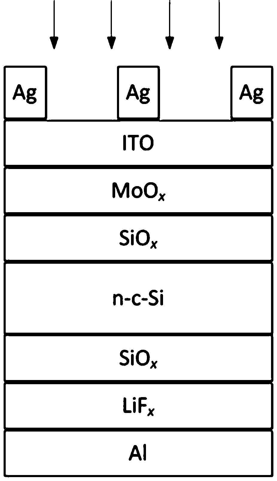
[0018] Such as figure 1 As shown, the solar cell structure described in this embodiment is divided into several layers, from top to bottom: Ag / ITO / MoO x / SiO y / n-c-Si / SiO y / LiF z / Al, where Ag is metallic silver, ITO is tin-doped indium oxide transparent conductive film, MoO x It is molybdenum oxide, x=2.3~3.0, SiO y It is silicon oxide, y=1.5~2.0, n-c-Si is n-type single crystal silicon, LiF z It is lithium fluoride, z=0.8~1.0, and Al is metal aluminum.

[0019] The preparation method is as follows: firstly, chemically treat the surface of the single crystal silicon wafer to remove the damaged layer and remove surface contamination impurities, and then use the nitric acid oxidation method to grow a layer of ultra-thin SiO on the front and rear surfaces of the silicon wafer. y layer (1.0-1.3nm), and then sequentially grow MoO on the front side of the silicon wafer x , ITO, Ag, and LiF are grown sequentially on the back of the silicon wafer x and Al.

[0020] Specifi...


PUM

PropertyMeasurementUnit
Thicknessaaaaaaaaaa

Abstract

The invention discloses a selective contact crystalline silicon heterojunction solar cell and a preparation method thereof. The structure of the solar cell is divided into a plurality of layers from top to bottom: Ag/ITO/MoOx/SiOy/n-c-Si/SiOy/LiFz/Al. During preparation, an ultra-thin SiOy layer (1.0-1.3 nm) grows on the front and rear surfaces of a silicon wafer through the nitric acid oxidationprocess. After that, MoOx, ITO and Ag sequentially grow on the front surface of the silicon wafer, while LiFx and Al sequentially grow on the back surface of the silicon wafer. According to the invention, the selective separation of photogenerated carriers is realized through bending the heterojunction energy band of MoOx/c-Si and LiFz/c-Si respectively based on the high-work function characteristics of MoOx and the low-work function characteristics of LiFz.

Description

technical field [0001] The invention belongs to the field of solar cells, and relates to a novel crystalline silicon heterojunction solar cell structure with selective contact and a preparation method thereof. Background technique [0002] In solar cells, efficient separation, transport, and collection of photogenerated charge carriers (electron-hole pairs) are crucial to improving the overall performance of the cell. The current industrial mass-produced crystalline silicon solar cells obtain p-n junctions through the diffusion of phosphorus on the surface of p-type silicon wafers. The front and rear electrodes are collected. Traditional crystalline silicon heterojunction solar cells mainly use hydrogenated amorphous silicon (a-Si:H) as the doped layer, but a-Si:H has a high density of defect states and a narrow band gap (~1.8 eV), even with a thickness of only a few nanometers in solar cells, leads to significant parasitic light absorption in the ultraviolet and visible r...

Claims


Application Information

Patent Timeline
IPC IPC(8): H01L31/074H01L31/18
CPCH01L31/074H01L31/18Y02E10/50Y02P70/50
Inventor 黄仕华王佳黄玉清芮哲
Owner ZHEJIANG NORMAL UNIVERSITY
Why Eureka
Try Eureka