Textured substrate capable of enhancing electrical stability of flexible device in mechanical stress
A technology of mechanical stress and flexible electronic devices, applied in semiconductor devices, circuits, photovoltaic power generation, etc., can solve problems such as various loads, thermal expansion coefficient material property mismatch, etc., achieve significant technical economy, reduce failure behavior, The effect of reducing the cost of preparation and processing
- Summary
- Abstract
- Description
- Claims
- Application Information
AI Technical Summary
Problems solved by technology
Method used
Image
Examples
preparation example Construction
[0062] The preparation method of the flexible ZnO nanowire ultraviolet detector and the detection of its electrical stability under mechanical stress are characterized in that it comprises the following steps:
[0063] Step 1: Glue the cleaned textured and smooth flexible substrates with a size of 1cm×1cm on the pre-prepared silicon wafer with high temperature resistant double-sided adhesive, divide the samples into two groups, each group contains a texture Substrate and a smooth substrate, and rinse again, and then dry the sample;
[0064] Step 2: patterning the entire substrate by photolithography;
[0065] Step 3: On the patterned sample, the ZnO film was sputtered by radio frequency magnetron sputtering. In order to compare the combination of the ZnO film and the two flexible substrates under different sputtering powers, that is, different ZnO film qualities, the first group The sputtering power of the sample is 150W, and the sputtering power of the second group of sample...
Embodiment 1
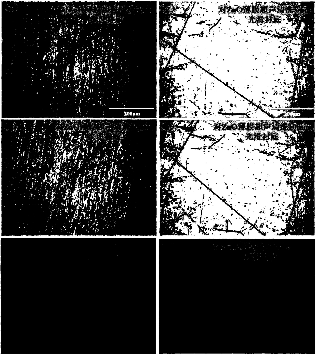
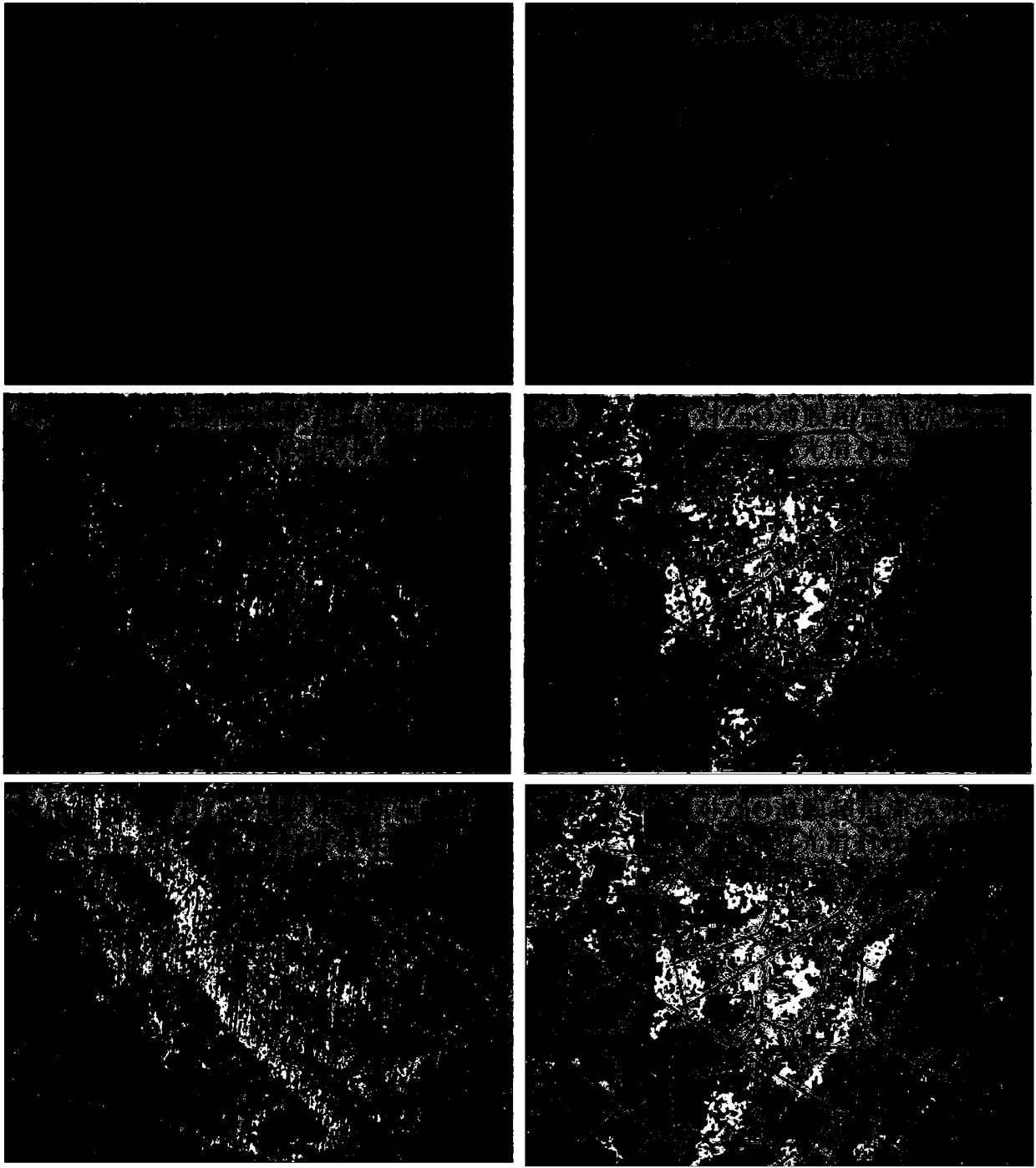
[0074] Ultrasonic cleaning was used to test the bonding strength of textured and smooth substrates to ZnO thin films:
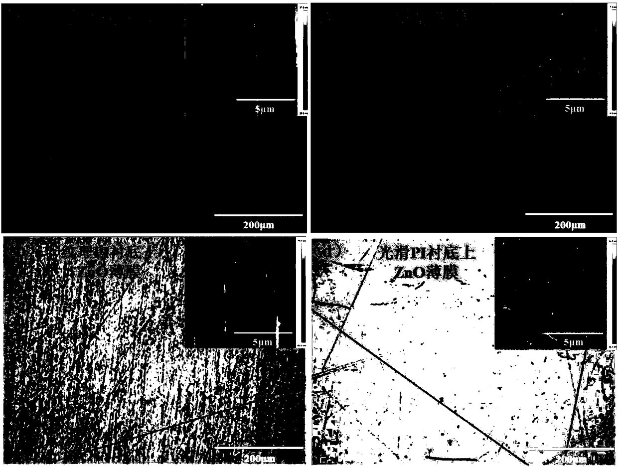
[0075] The height difference between adjacent peaks and troughs on the textured PI substrate surface is 10-100nm, the distance between two adjacent peaks or two troughs is 50-500nm, and the roughness Ra is 6.54 in the range of 10μm×10μm. nm, such as figure 1 (a). The surface of the smooth substrate used is within the range of 10 μm × 10 μm, and the roughness Ra is 1.18 nm, such as figure 1 (c).
[0076] The cleaned textured and smooth flexible PI substrates of 1cm×1cm in size and 100μm in thickness were glued to the pre-prepared silicon wafer with high-temperature-resistant double-sided adhesive, and cleaned again, and then the samples were dried and passed through radio frequency magnetron sputtering. A 130nm thick ZnO film was sputtered with a sputtering power of 150W. The images under the optical microscope and the AFM images of the two PI substrates us...
PUM
| Property | Measurement | Unit |
|---|---|---|
| Roughness | aaaaa | aaaaa |
| Thickness | aaaaa | aaaaa |
| Size | aaaaa | aaaaa |
Abstract
Description
Claims
Application Information


