Monocrystalline wafer production system and production process thereof

A monocrystalline silicon wafer and production system technology, applied in the direction of manufacturing tools, stone processing equipment, metal processing equipment, etc., can solve problems such as low chamfering efficiency, burnt monocrystalline silicon wafers, and high labor intensity, and achieve improved chamfering Efficiency, improvement of tooling efficiency, and high degree of automation

Active Publication Date: 2018-08-17
四川雅吉芯电子科技有限公司
View PDF7 Cites 7 Cited by
  • Summary
  • Abstract
  • Description
  • Claims
  • Application Information

AI Technical Summary

Problems solved by technology

However, this method needs to manually hold the grinding wheel for grinding, which has the defects of high labor intensity and low chamfering efficiency
In addition, frequent operation of the vacuum suction cup is required for each loading and unloading, which further increases the labor intensity of workers and reduces the chamfering efficiency
[0006] Among them, in the mid-term grinding process, the upper surface of the single crystal silicon wafer is usually ground first with a grinding disc, and then turned over 180° to grind the other side, which undoubtedly increases the labor intensity of the workers, and there is also discontinuous grinding. Defects reduce the grinding efficiency
In addition, the monocrystalline silicon wafer and the grinding disc belong to dry friction, which will easily cause the surface of the grinding disc to heat up and be damaged, and the heat will also burn the monocrystalline silicon wafer.

Method used


Image

  • Monocrystalline wafer production system and production process thereof
  • Monocrystalline wafer production system and production process thereof
  • Monocrystalline wafer production system and production process thereof

Examples


Embodiment Construction

[0041] The present invention will be further described below in conjunction with accompanying drawing, protection scope of the present invention is not limited to the following:

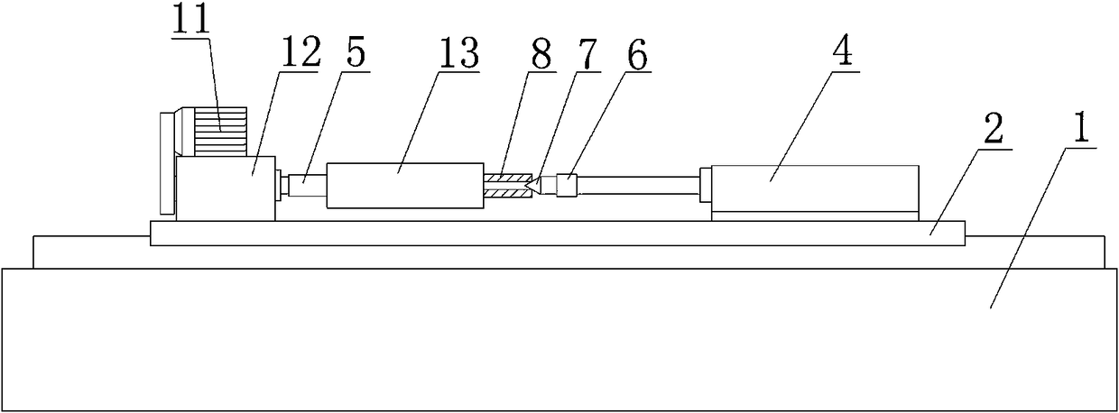
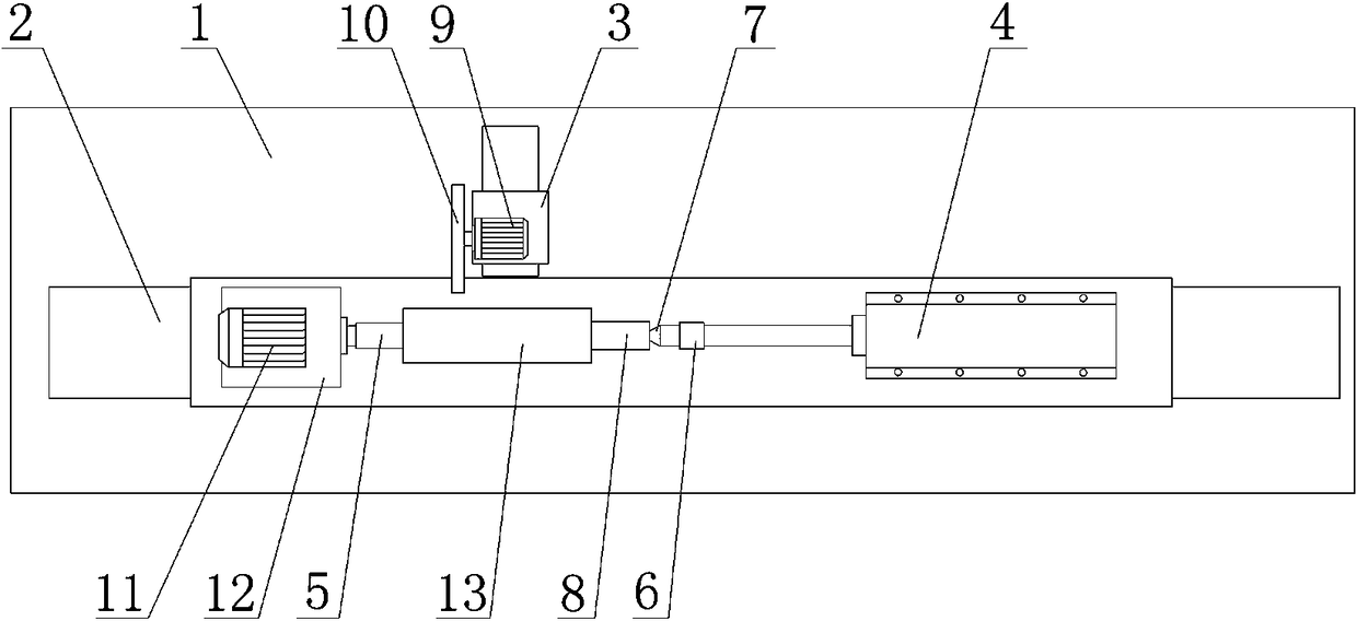
[0042] Such as Figure 1~13 Shown, a kind of monocrystalline silicon wafer production system, it comprises roller mill, slicing device, chamfering device, grinder and cleaning tank;

[0043] Such as Figure 1~2 As shown, the rolling mill includes a fuselage 1, a horizontal hydraulic slide table 2 and a vertical hydraulic slide table 3 arranged on the top of the fuselage 1, and the top surface of the horizontal hydraulic slide table 2 is located at its left and right ends respectively. A power mechanism and a horizontal oil cylinder 4 are provided, the output end of the power mechanism is connected with a rotating shaft 5, the end of the piston rod of the horizontal oil cylinder 4 is rotatably mounted with a shaft sleeve 6, and the left end surface of the shaft sleeve 6 is provided with a conical hea...


PUM


Abstract

The invention discloses a monocrystalline wafer production system which comprises a roller mill, a slicing device, a chamfering device, a grinding miller and a cleaning tank. The invention further discloses a monocrystalline wafer production process. The monocrystalline wafer production system and the monocrystalline wafer production process provided by the invention have the beneficial effects that the roll-milling accuracy is high, the clamping of monocrystalline silicon rods can be quickly realized, the monocrystalline silicon rods with different lengths can be roll-milled and can be slicedinto multiple monocrystalline wafers at one time, the automatic centering is realized, the chamfering efficiency is improved, an automation degree is high, the multiple monocrystalline wafers can beground at one time, the grinding efficiency is high, and the cleaning efficiency is high.

Description

technical field [0001] The invention relates to the technical field of monocrystalline silicon wafer production, in particular to a monocrystalline silicon wafer production system and a production process thereof. Background technique [0002] As an important semiconductor material, single crystal silicon has good electrical properties and thermal stability, and it has replaced other semiconductor materials soon after it was discovered and utilized. Silicon material has become the most widely used semiconductor material because of its high temperature resistance and radiation resistance, and is especially suitable for making high-power devices. Most integrated circuit semiconductor devices are made of silicon materials. Among the methods for manufacturing silicon single crystals with good performance, the Czochralski method for growing silicon single crystals has relatively simple equipment and processes, and is easy to realize automatic control. After the Czochralski monoc...

Claims


Application Information

Patent Timeline
IPC IPC(8): B24B5/04B24B9/06B24B37/08B24B37/34B24B47/06B24B47/12B24B47/20B24B57/02B28D5/00B28D5/04B08B3/04B08B3/12
CPCB08B3/044B08B3/123B24B5/04B24B9/06B24B37/08B24B37/34B24B47/06B24B47/12B24B47/20B24B57/02B28D5/007B28D5/0082B28D5/045
Inventor 王全文杨蛟李鹭
Owner 四川雅吉芯电子科技有限公司
Why Eureka
Try Eureka