Mosfet with semi-insulating region and its preparation method

A technology of semi-insulating and insulating gate layers, which is applied in semiconductor/solid-state device manufacturing, semiconductor devices, electrical components, etc., can solve the problems of low avalanche breakdown tolerance of MOSFETs, reduce leakage current, improve UIS robustness, and improve The effect of breakdown voltage

Active Publication Date: 2021-02-02
ANHUI UNIVERSITY OF TECHNOLOGY
View PDF7 Cites 0 Cited by
  • Summary
  • Abstract
  • Description
  • Claims
  • Application Information

AI Technical Summary

Problems solved by technology

[0007] Aiming at the problem of low avalanche breakdown tolerance of MOSFET in the prior art, the present invention provides a MOSFET containing a semi-insulating region and a preparation method thereof

Method used


Image

  • Mosfet with semi-insulating region and its preparation method
  • Mosfet with semi-insulating region and its preparation method
  • Mosfet with semi-insulating region and its preparation method

Examples


Embodiment 1

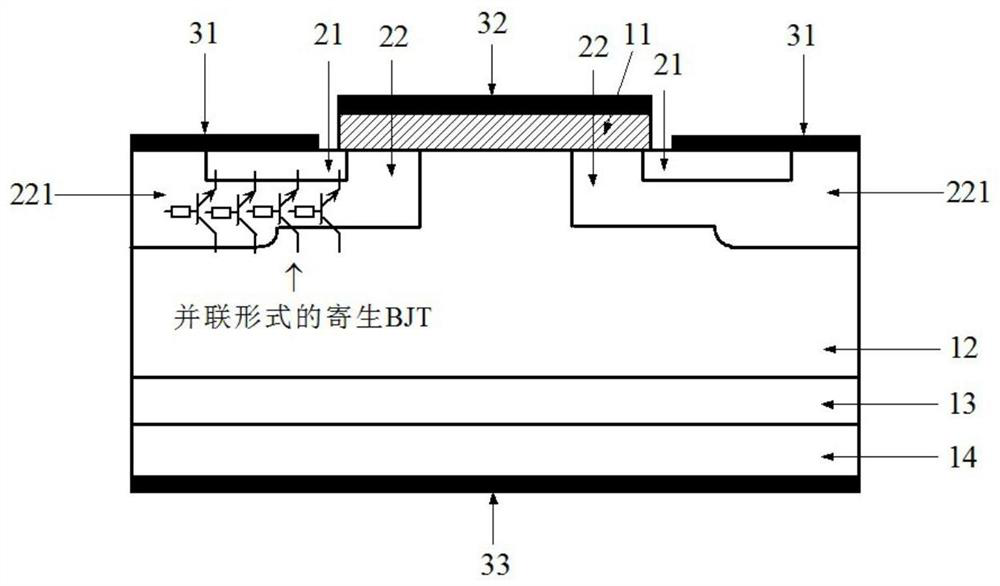
[0046] The MOSFET containing the semi-insulating region of this embodiment, such as image 3 As shown, the semi-insulating region 222 is located below the base region 22 doped with the semiconductor of the first conductivity type and the source region 21 doped with the semiconductor of the second conductivity type arranged side by side. Type semiconductor doped drift layer 12 contacts.

[0047] By setting the semi-insulating region 222, the area where the MOSFET parasitic BJT exists is greatly reduced, thereby greatly reducing the number of parasitic BJT, only a small amount of parasitic BJT still exists in the shallow base area, but due to the great reduction in the number of parasitic BJT , thereby reducing the current in the MOSFET under UIS conditions, limiting the temperature rise, and increasing the avalanche breakdown time of the MOSFET from the theoretical 8 microseconds to 38 microseconds, increasing the time integral of the voltage to the current, and improving the a...

Embodiment 2

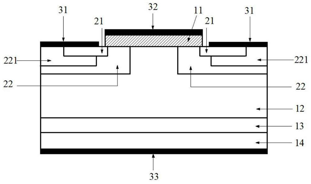
[0052] The MOSFET containing the semi-insulating region of this embodiment, such as image 3 As shown, a further improvement is made on the basis of Embodiment 1. The width of the semi-insulating region 222 is equal to the sum of the widths of the base region 22 doped with the semiconductor of the first conductivity type and the source region 21 doped with the semiconductor of the second conductivity type. The width ratio of the base region 22 doped with the first conductivity type to the source region 21 doped with the second conductivity type is 1:1-3. For specific applications, values ​​such as 1:1; 1:2; 1:3; 1:1.5; 1:2.8 can be selected.

[0053] Precisely controlling the effective channel length of the MOSFET does not change due to the introduction of the semi-insulating region 222, ensuring that parameters such as the threshold voltage, on-resistance, transconductance, and output characteristics of the MOSFET do not change due to the introduction of the semi-insulating r...

Embodiment 3

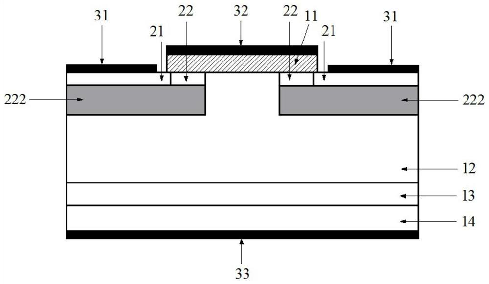
[0055] The MOSFET containing the semi-insulating region of this embodiment, such as image 3 As shown, a further improvement is made on the basis of Embodiments 1 and 2, and the depth of the semiconductor-doped base region 22 is consistent with that of the second conductivity type semiconductor-doped source region 21 . Ensure that the channel carriers are transported smoothly without "crossing the ridge", otherwise the formed abrupt junction will form a potential barrier for the carriers, which is not conducive to the normal operation of the device.


PUM


Abstract

The invention discloses a MOSFET containing a semi-insulating region and a preparation method thereof, and belongs to the technical field of high-voltage power electronics. The semi-insulating region is located under the base region doped with the first conductive type semiconductor and the source region doped with the second conductive type semiconductor arranged side by side, and the bottom and sides of the semi-insulating region are both connected with the drift layer doped with the second conductive type semiconductor. touch. The semi-insulating region is firstly ion-implanted with impurities of the second conductivity type to achieve counter-doping to form an electrically neutral layer, and then rely on ion-implanted amphoteric impurity elements to form a semi-insulating region, and the shallow base region relies on ion implantation above the semi-insulating region. Impurities of conductivity type are formed. By reducing the area where the parasitic transistor of the MOSFET exists, the "hot run" problem caused by the current runaway caused by the turn-on of the parasitic transistor of the conventional MOSFET under UIS conditions can be solved, which can significantly improve the avalanche resistance, robustness, ability to resist large currents, and shocks. Breakthrough voltage and reliability.

Description

technical field [0001] The invention relates to the technical field of high-voltage power electronics, relates to a semiconductor power device, in particular to a MOSFET containing a semi-insulating region and a preparation method thereof. Background technique [0002] With the continuous improvement of the performance requirements of power conversion devices, higher requirements are put forward for power MOS transistor devices that undertake power conversion functions, one of which is to have high avalanche tolerance in the unclamped inductive load switching process (UIS) , that is, it has a high ability to resist UIS avalanche breakdown. This is because the energy stored in the inductive load under UIS conditions is required to be fully released by the power MOS transistor when it is turned off. At this time, the high current stress in the circuit is very high. It is easy to cause device failure, so the level of avalanche breakdown resistance is one of the important indica...

Claims


Application Information

Patent Timeline
Patent Type & Authority Patents(China)
IPC IPC(8): H01L29/78H01L29/06H01L21/336
CPCH01L29/0619H01L29/66712H01L29/7802H01L29/66068H01L29/1608H01L29/167H01L29/0653
Inventor 周郁明王兵
Owner ANHUI UNIVERSITY OF TECHNOLOGY
Why Eureka
Try Eureka