A kind of preparation method of coplanar waveguide structure micro-LED

A coplanar waveguide and area technology, applied in semiconductor devices, electrical components, circuits, etc., can solve the problems of high-frequency signal feeding of array LEDs, heat dissipation of high-power LEDs, etc., to break through power shortage, optimize heat dissipation performance, and improve heat dissipation performance effect

Active Publication Date: 2021-03-23
PEKING UNIV
View PDF12 Cites 0 Cited by
  • Summary
  • Abstract
  • Description
  • Claims
  • Application Information

AI Technical Summary

Problems solved by technology

[0005] The invention provides a method for preparing a micro-LED for communication with a coplanar waveguide structure, which solves the problem of high-frequency signal feed-in of array LEDs and the problem of heat dissipation of high-power LEDs

Method used


Image

  • A kind of preparation method of coplanar waveguide structure micro-LED
  • A kind of preparation method of coplanar waveguide structure micro-LED
  • A kind of preparation method of coplanar waveguide structure micro-LED

Examples


Embodiment Construction

[0030] The present invention will be further described below in conjunction with the accompanying drawings and specific embodiments.
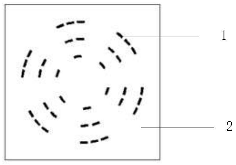
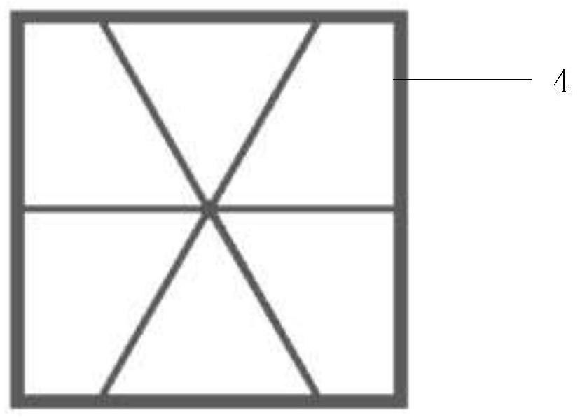
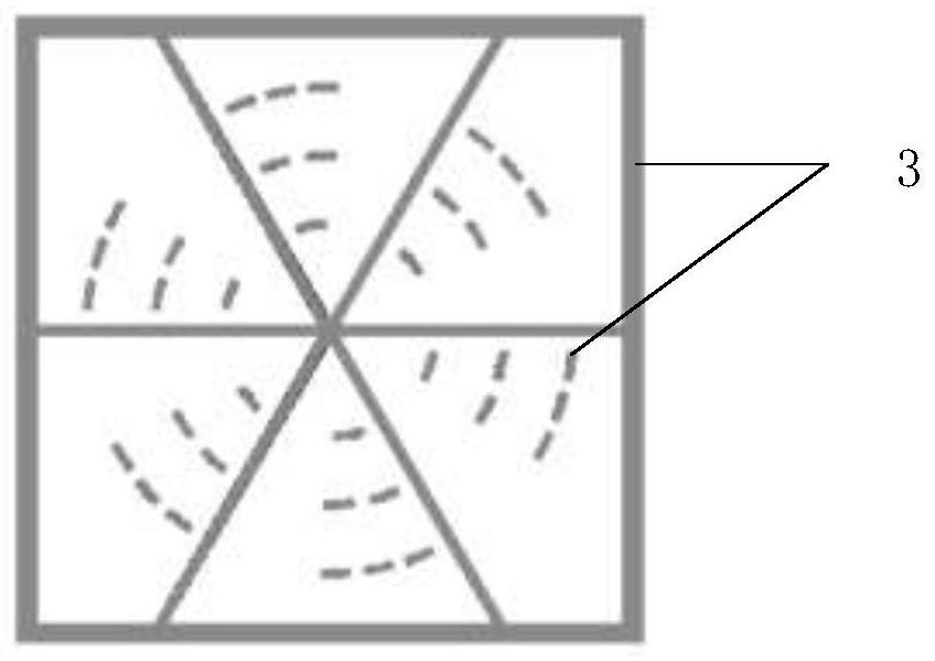
[0031] First, determine the area of ​​a single micron LED in the array and the total number of LEDs according to the final power requirement, where the area of ​​a single LED is 888um 2 , the total number of LEDs is 36. By simulating heat distribution, current distribution, and high-frequency signal feed-in conditions, and then according to the simulation effect, optimize and design six LED mesa areas divided by isolation areas, as well as the electrode structure.

[0032] After the sapphire substrate LED epitaxial wafer is pickled, organically cleaned, rinsed with deionized water until the surface is free of contamination and oxide layer and dried, a layer of ITO is evaporated as a current spreading layer;

[0033] The photoresist is coated by the coater, and through exposure and development, a number of radially distributed fan-shaped mesa a...


PUM


Abstract

The invention provides a preparing method of a coplanar waveguide structure micrometer LED, and belongs to the field of a photoelectric device oriented to a visible light communication LED. The preparing method comprises the steps of simulating optimized chip distribution and an electrode structure, then burying and controlling electronic beam evaporation conditions through imaging in the chip technology process and finally, achieving a coplanar waveguide structure in a chip to make a high-frequency signal capable of being fed into each LED terminal in an array. The preparing method is compatible to traditional LED manufacturing technology and is also simple and reliable, so that the high-frequency signal is effectively fed, and the bandwidth of the large power chip is increased; meanwhile, the chip is welded to a heat conducting substrate, the cooling performance of the large power chip can be greatly improved, and the reliability of the large power chip is effectively improved.

Description

technical field [0001] The invention relates to the field of optoelectronic devices facing visible light communication LEDs, and relates to a preparation method of a high-bandwidth micro-LED with a waveguide structure. Background technique [0002] In recent years, with the development of science and technology, LED is rapidly replacing traditional fluorescent lamps and other light sources to become the mainstream indoor lighting source. This is due to the fact that LED lighting devices are a green lighting source with higher efficiency and longer life. Compared with traditional lighting sources such as incandescent lamps and fluorescent lamps, high-power white LEDs not only have higher luminous efficiency, but also have the characteristics of high-speed modulation, so LEDs can realize wireless optical transmission of data while lighting, that is, Li-Fi. Visible light communication technology has the advantages of rich spectrum resources, no electromagnetic pollution, and s...

Claims


Application Information

Patent Timeline
Patent Type & Authority Patents(China)
IPC IPC(8): H01L33/00H01L33/64
CPCH01L33/005H01L33/64
Inventor 康香宁李诚诚陈志忠焦飞冯玉龙詹景麟于彤军吴洁君沈波
Owner PEKING UNIV
Why Eureka
Try Eureka