Deep silicon etching method based on SOG wafers

A deep silicon etching and wafer technology, which is used in the process of producing decorative surface effects, decorative arts, gaseous chemical plating, etc. Etch depth, unrealizable bulk silicon structure, etc.

Active Publication Date: 2018-08-24
TSINGHUA UNIV
View PDF10 Cites 1 Cited by
  • Summary
  • Abstract
  • Description
  • Claims
  • Application Information

AI Technical Summary

Problems solved by technology

However, there is a problem in the process that the etching rate decreases with the narrowing of the trench width. This phenomenon is also called the lag effect, and sometimes the etching rate in the narrow trench is zero. Therefore, it is difficult to control the etching side. Wall verticality and etch depth
These problems seriously affect the use of high aspect ratio etching technology, and many bulk silicon structures cannot be realized

Method used


Image

  • Deep silicon etching method based on SOG wafers
  • Deep silicon etching method based on SOG wafers
  • Deep silicon etching method based on SOG wafers

Examples


Embodiment 1

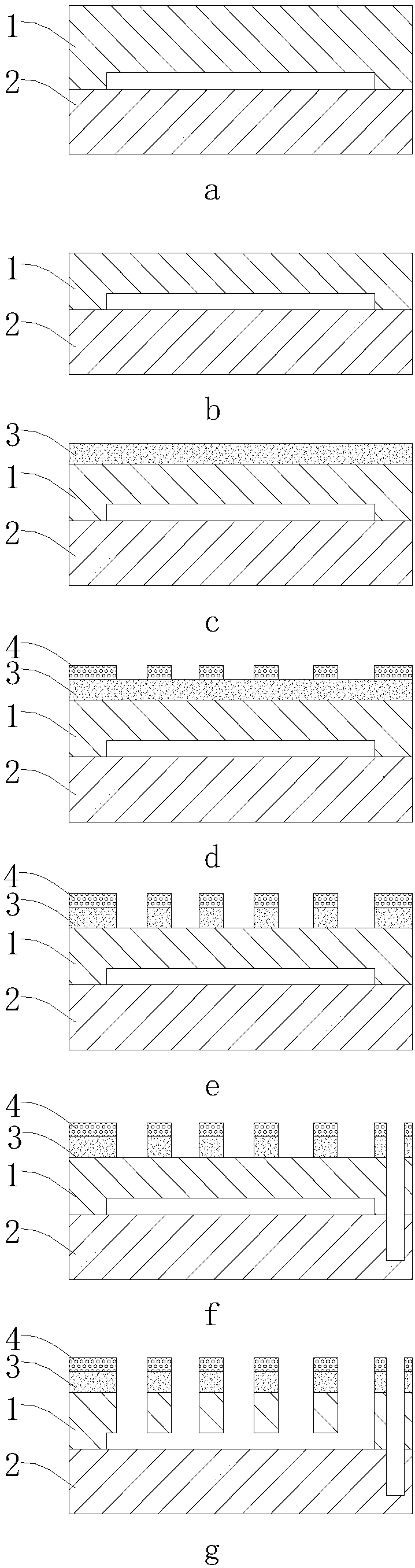
[0042] process such as figure 1 shown.

[0043] a. Silicon structure layer-glass substrate bonding:

[0044] The silicon structure layer 1 with anchor points and the glass substrate 2 with conductive leads are bonded to complete the silicon structure layer-glass substrate bonding process to form an SOG wafer with a diameter of 6 inches. The parameters of the bonding process are: the temperature of the process chamber is 350°C, the pressure of the process chamber is 5×10⁻⁴mbar, the bonding pressure is 600N, the bonding voltage is 800V, and the bonding time is 90s.

[0045] b. Thinning the silicon structure layer:

[0046] Using a KOH solution with a temperature of 80° C. and a concentration of 30%, soaking the silicon structure layer for 1200 min, and thinning the silicon structure layer 1 of the SOG wafer to a required thickness of 80 μm. After soaking, rinse with water for 5 times, and then use a spin dryer to spin dry at a speed of 2000 rpm for 5 minutes, and fill the spi...

Embodiment 2

[0065] process such as figure 1 shown.

[0066] a. Silicon structure layer-glass substrate bonding:

[0067] The silicon structure layer 1 with anchor points and the glass substrate 2 with conductive leads are bonded together to form a 6-inch diameter SOG wafer. The parameters of the bonding process are: the temperature of the process chamber is 350°C, the pressure of the process chamber is 5×10⁻⁴mbar, the bonding pressure is 600N, the bonding voltage is 800V, and the bonding time is 90s.

[0068] b. Thinning the silicon structure layer:

[0069] Using a KOH solution with a temperature of 80° C. and a concentration of 30%, soaking the silicon structure layer for 1200 min, and thinning the silicon structure layer 1 of the SOG wafer to a required thickness of 80 μm. After soaking, rinse with water for 5 times, and then use a spin dryer to spin dry at a speed of 2000 rpm for 5 minutes, and fill the spin dryer with hot nitrogen at 50°C and 20 LPM.

[0070] c. Deposition of SiO...

Embodiment 3

[0088] process such as figure 1 shown.

[0089] a. Silicon structure layer-glass substrate bonding:

[0090] The silicon structure layer 1 with anchor points and the glass substrate 2 with conductive leads are bonded to complete the silicon structure layer-glass substrate bonding process to form an SOG wafer with a diameter of 6 inches. The parameters of the bonding process are: the temperature of the process chamber is 350°C, the pressure of the process chamber is 5×10⁻⁴mbar, the bonding pressure is 600N, the bonding voltage is 800V, and the bonding time is 90s.

[0091] b. Thinning the silicon structure layer:

[0092] Using a KOH solution with a temperature of 80° C. and a concentration of 30%, soaking the silicon structure layer for 1200 min, and thinning the silicon structure layer 1 of the SOG wafer to a required thickness of 80 μm. After soaking, rinse with water for 5 times, and then use a spin dryer to spin dry at a speed of 2000 rpm for 5 minutes, and fill the spi...


PUM

PropertyMeasurementUnit
Etching depthaaaaaaaaaa

Abstract

The invention relates to a deep silicon etching method based on SOG wafers. The method comprises the steps of providing a SOG wafer and placing the SOG wafer on a flat plate; forming a hard mask layeron the silicon structure layer of the SOG wafer; forming a photo-resist layer on the hard mask layer, exposing and developing to expose one part of the hard mask layer; etching the exposed part of the hard mask layer to expose one part of the silicon structure layer; and subjecting the exposed part of the silicon structure layer to deep-induction coupling plasma dry etching in a chamber. The deep-induction coupling plasma dry etching comprises a first etching stage and a second etching stage. The first etching stage comprises a first passivation step, a first pre-etching step and a first etching step, wherein the first passivation step, the first pre-etching step and the first etching step are carried out circularly. The second etching stage comprises a second passivation step, a second pre-etching step and a second etching step, wherein the second passivation step, the second pre-etching step and the second etching step are carried out circularly. The pressure in the first etching step and the pressure in the second etching step are respectively 30 mTorr to 40 mTorr. The etching time and the radio frequency power at the flat plate in the first etching step and the second etchingstep are gradually increased along with the increase of the cycle period.

Description

technical field [0001] The invention relates to the technical field of MEMS manufacturing technology, in particular to a deep silicon etching method based on SOG wafers. Background technique [0002] Micro-electromechanical system sensors are more and more widely used in the fields of automobiles, mobile phones and smart wearable devices, and MEMS technology with bulk silicon technology as the core is developing particularly rapidly. The development of high aspect ratio silicon etching technology has greatly improved the sensitivity of micro sensors and actuators. Compared with surface silicon technology, the bulk silicon technology with deep silicon etching technology as the core can obtain larger detection capacitance and more sensitive The quality block structure improves the resolution and sensitivity of the MEMS sensor. [0003] The bulk silicon process based on the SOG wafer (full name silicon structure layer-glass substrate bonded wafer) is a key process in the proce...

Claims


Application Information

Patent Timeline
IPC IPC(8): H01L21/3065B81C1/00
CPCB81C1/00531B81C2201/0132H01L21/30655
Inventor 阮勇尤政刘琛琛
Owner TSINGHUA UNIV
Why Eureka
Try Eureka