Electrical bistable characteristics-based single-layer polymer electric memory and manufacturing method thereof

A technology of electrical memory and photoelectric polymer, which is applied in the manufacture of semiconductor/solid-state devices, electrical solid-state devices, circuits, etc., can solve the problems of difficulty in realizing large-area flexible storage, unfavorable environmental impact, and high manufacturing costs, and achieve large-area flexibility. The effect of storage, simple process and simple structure

Inactive Publication Date: 2018-08-24
WUHAN INSTITUTE OF TECHNOLOGY
View PDF16 Cites 2 Cited by
  • Summary
  • Abstract
  • Description
  • Claims
  • Application Information

AI Technical Summary

Problems solved by technology

Among them, small molecule materials need to use a thermal evaporation process with high manufacturing costs, so there is a lot of material waste, and it is difficult to achieve large-area flexible storage. In addition, a toxic atmosphere is often generated during the film growth process, which is not good for the environment.

Method used


Image

  • Electrical bistable characteristics-based single-layer polymer electric memory and manufacturing method thereof
  • Electrical bistable characteristics-based single-layer polymer electric memory and manufacturing method thereof
  • Electrical bistable characteristics-based single-layer polymer electric memory and manufacturing method thereof

Examples


Embodiment 1

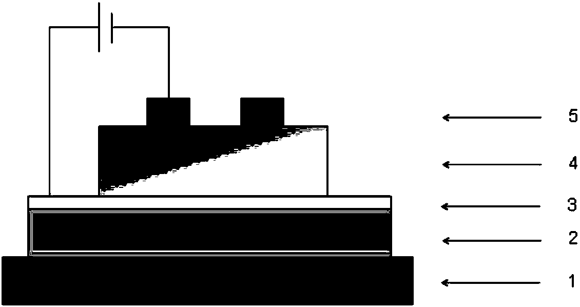
[0042] First, the ITO on the ITO glass is photolithographically formed into electrodes with a width of 4 mm and a length of 30 mm, and then ultrasonically cleaned with acetone, isopropanol, glass cleaner, and deionized water, and dried with nitrogen. Plasma treatment for 4-10 minutes. Spin-coat PEDOT:PSS polymer aqueous solution on the cleaned ITO electrode, and vacuum bake at a constant temperature of 50-150°C for 0.5-3 hours to form a hole injection layer (also known as an anode buffer layer). PEDOT:PSS is mainly used to modify the ITO electrode and form the real anode of the device together with ITO. Then spin-coat the photoelectric polymer MEH-PPV xylene solution on the well-formed PEDOT:PSS, and vacuum bake at a constant temperature of 50-200°C for 10-40 minutes to form a photoelectrically active functional layer with a smooth surface and no defects. Finally, transfer the sample to the coating equipment, in a vacuum of (1-5)×10 -4 Under the condition of Pa, the metal Au...

Embodiment 2

[0046] The process and parameters of embodiment 2 are basically the same as those of embodiment 1, except that the top electrode is replaced by 50-300nm Au with 50-300nm Al.

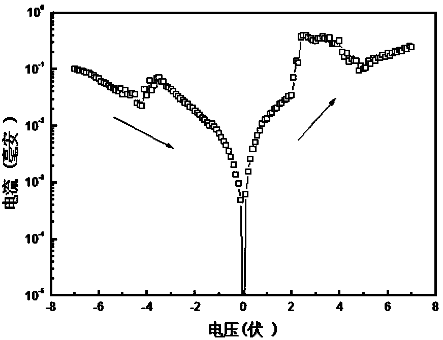
[0047] The memory has an effective area of ​​16 square millimeters. Figure 4 Its typical and representative current and voltage scanning characteristic curves are given. It can be seen from the figure that the device also exhibits a sudden change in current when scanning from negative to positive. This sudden change in current can be used in the manufacture of electrical switching memory devices.

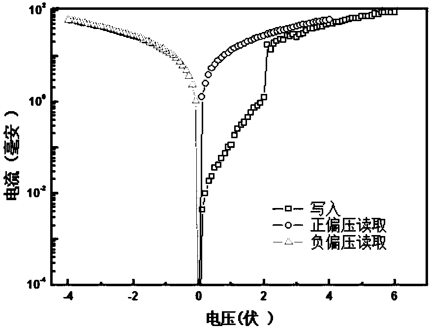
[0048] Figure 5 A description of the data read and write process of the device is given, and the current switch ratio is 90. Under normal temperature and pressure, the current of a simple packaged device does not change significantly even if it is switched more than one million times.

Embodiment 3

[0050] The process and parameters of embodiment 3 are basically the same as those of embodiment 1, except that the top electrode is replaced by 50-300nm Au with 10-50nm Ba and 40-250nm Al, wherein the evaporation rate of Ba is controlled at 0.1 -0.5 nm / s, the evaporation rate of Al is controlled at 0.2-2 nm / s.

[0051] The memory has an effective area of ​​16 square millimeters. Figure 6 The typical representative current-voltage sweep characteristic curve of the polymer electrical storage device is given. It can be seen from the figure that: the voltage sweep changes from negative bias to positive bias, and then back to negative bias, and the device shows a sudden change in current.

[0052] Figure 7 A description of the current-voltage relationship before and after the abrupt change of the device current is given. Taking the negative bias interval as an example, the logarithm of the current and voltage in the high conductance state presents a linear relationship with a s...


PUM

PropertyMeasurementUnit
thicknessaaaaaaaaaa
thicknessaaaaaaaaaa
thicknessaaaaaaaaaa

Abstract

The invention relates to an electrical bistable characteristics-based single-layer polymer electric memory and a manufacturing method thereof. The electric memory comprises a glass substrate or a PETsubstrate or a PI substrate, an ITO bottom electrode, a PEDOT: PSS hole injection layer, an MEH-PPV or PFO or P-PPV photoelectric polymer active functional layer and a metal top electrode. All the above layers are formed through spin coating or evaporation. The electric memory provided by the invention is simple in structure, and has excellent electrical bistable characteristics, storage responsespeed and stability. During the reading and writing process, the electric memory is low in false reading rate. Even when the electric memory is switched on and off for over million of times, the current of the electric memory is not obviously changed.

Description

technical field [0001] The invention relates to the technical field of electric storage materials, in particular to an electric bistable single-layer polymer memory based on MEH-PPV, PFO and P-PPV and a preparation method thereof. Background technique [0002] The rapid growth of data generated by the modern information society requires that the memory should have a larger storage capacity. Although the widely used silicon memory has the characteristics of fast storage, expensive manufacturing equipment, complex photolithography process and peripheral transistor drive circuit increase the manufacturing cost, and the limited area of ​​silicon wafer and two-dimensional (2D) process limit the storage capacity. Capacity, can no longer meet the requirements of large-capacity information storage and portability in the information age. People usually use physical means such as increasing the integration density of memory cells to increase the storage capacity of the memory, but th...

Claims


Application Information

Patent Timeline
Patent Type & Authority Applications(China)
IPC IPC(8): H01L51/05H01L51/30H01L51/40
CPCH10K71/12H10K85/10H10K10/50
Inventor 石胜伟李文婷
Owner WUHAN INSTITUTE OF TECHNOLOGY
Why Eureka
Try Eureka