Gan-based light-emitting diode with nanoscale silicon dioxide grating passivation layer and its processing method

A technology for light-emitting diodes and processing methods, which is applied to semiconductor devices, electrical components, circuits, etc., can solve the problems of external quantum efficiency and shortening of lifespan of light-emitting diodes, so as to improve light extraction efficiency, reduce current concentration, and reduce leakage current. Effect

Active Publication Date: 2019-10-11
JIANGXI ZHAO CHI SEMICON CO LTD
View PDF4 Cites 2 Cited by
  • Summary
  • Abstract
  • Description
  • Claims
  • Application Information

AI Technical Summary

Problems solved by technology

In the horizontal structure light-emitting diode in this study, because the current spread in the horizontal direction is hindered by the steps, the current gathers near the electrode, the heat is concentrated, and the photons generated by recombination are easily absorbed by the electrode, resulting in a large external quantum efficiency and lifetime of the light-emitting diode. decrease

Method used


Image

  • Gan-based light-emitting diode with nanoscale silicon dioxide grating passivation layer and its processing method
  • Gan-based light-emitting diode with nanoscale silicon dioxide grating passivation layer and its processing method
  • Gan-based light-emitting diode with nanoscale silicon dioxide grating passivation layer and its processing method

Examples


Embodiment Construction

[0046] The technical scheme of the present invention will be further explained below in conjunction with the drawings.

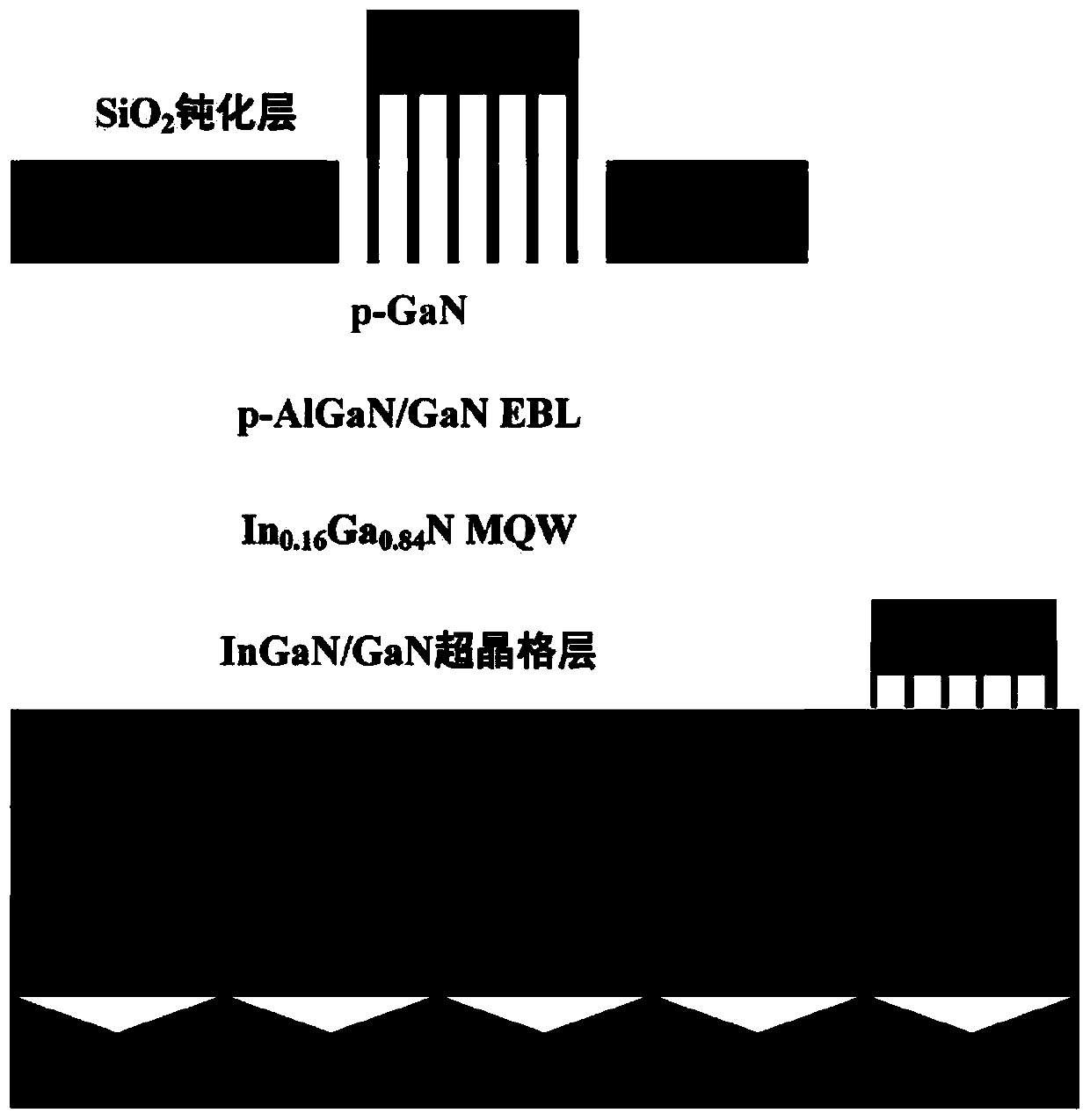
[0047] In this embodiment, GaN-based light-emitting diodes such as figure 1 As shown, it includes a patterned sapphire substrate 1, an AlN nucleation layer 2, a GaN buffer layer 3, an n-type GaN layer 4, an InGaN / GaN superlattice layer 5, In 0.16 Ga 0.84 N multiple quantum well layer 6, p-AlGaN / GaN electron blocking layer 7, p-type GaN layer 8, ITO layer 9, SiO 2 Passivation layer 10, P electrode and N electrode.

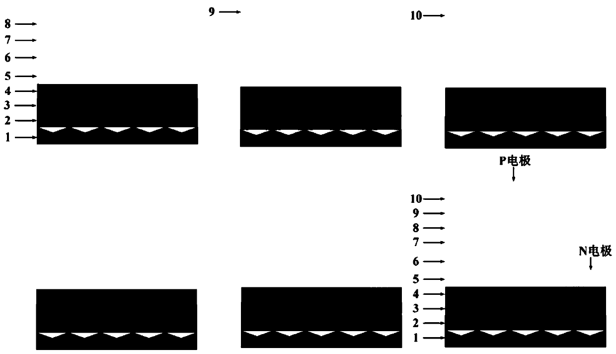
[0048] Reference to the manufacturing flow chart of the light emitting diode of the present invention figure 2 , The specific implementation steps are as follows:

[0049] (1) Place the cleaned c-plane patterned sapphire substrate 1 on a rotatable substrate;

[0050] (2) Draw the reaction chamber into 2.5×10 -3 Pa’s vacuum chamber, open to H 2 ;

[0051] (3) Under the condition of 1010℃, grow a 25nm thick AlN nucleation layer;

[0052] (4) At a temperature ...


PUM


Abstract

The invention discloses a GaN-based LED (Light Emitting Diode) having a nano-sized SiO2 grating passivation layer, and a processing method thereof. The GaN-based LED comprises a substrate and an epitaxial layer, wherein the epitaxial layer comprises an AIN nucleation layer, a GaN buffer layer, an n-type GaN layer, an InGaN / GaN superlattice layer, an In0.16Ga0.84N multiple quantum well layer, a p-AlGaN / GaN electronic blocking layer and a p-type GaN layer; a part of the epitaxial layer is etched to the n-type GaN layer, an un-etched part of the epitaxial layer forms a comb-shaped raised structure, the etched part of the epitaxial layer forms a comb-shaped groove structure matched with the comb-shaped raised structure; the p-type GaN layer is provided with an IOT layer, a SiO2 passivation layer and a P electrode thereon, the exposed n-type GaN layer after etching is provided with an N electrode, the SiO2 passivation layer is deposited between the N electrode and the n-type GaN layer, theSiO2 passivation layer is deposited on a sidewall of the raised structure; the ITO layer and the SiO2 passivation layer have graphical through-hole structures of which shapes are evenly distributed along the P electrode or the N electrode. The GaN-based LED of the invention has the beneficial effects that: the surface of the LED is protected, generation of a leakage current is limited, at the sametime, a current is expanded, current gathering is reduced, and luminous efficiency is improved.

Description

Technical field [0001] The invention belongs to the technical field of semiconductors, and relates to a nano-scale SiO 2 High-efficiency GaN-based light-emitting diode structure of grating passivation layer and processing method thereof. Background technique [0002] GaN-based light-emitting diodes, especially blue light-emitting diodes, are widely used in various devices due to their high luminous efficiency and long service life, involving the field of lighting, full-color display, and applications in biological, medical, chemical, and optical communications fields , Has great market potential. The improvement of its luminous efficiency and the extension of its service life are a topic of constant research. [0003] Because of its GaN (n=2.5), the total internal reflection that occurs at the interface between the smooth ITO (n=2.08) and the ambient air (n=1) limits the light extraction efficiency, and the intentional roughening of the LED surface can improve the LED’s Light ext...

Claims


Application Information

Patent Timeline
Patent Type & Authority Patents(China)
IPC IPC(8): H01L33/04H01L33/06H01L33/32H01L33/14H01L33/12H01L33/20H01L33/00
Inventor 周圣军赵杰
Owner JIANGXI ZHAO CHI SEMICON CO LTD
Why Eureka
Try Eureka