Solar cell passivation film, rear passivation solar cell and preparation method thereof
A solar cell and backside passivation technology, applied in the field of solar cells, can solve the problems of high cost and difficult passivation film preparation process, and achieve the effects of improving filling factor, lowering the threshold of preparation technology, and improving conversion efficiency.
- Summary
- Abstract
- Description
- Claims
- Application Information
AI Technical Summary
Problems solved by technology
Method used
Image
Examples
Embodiment 1
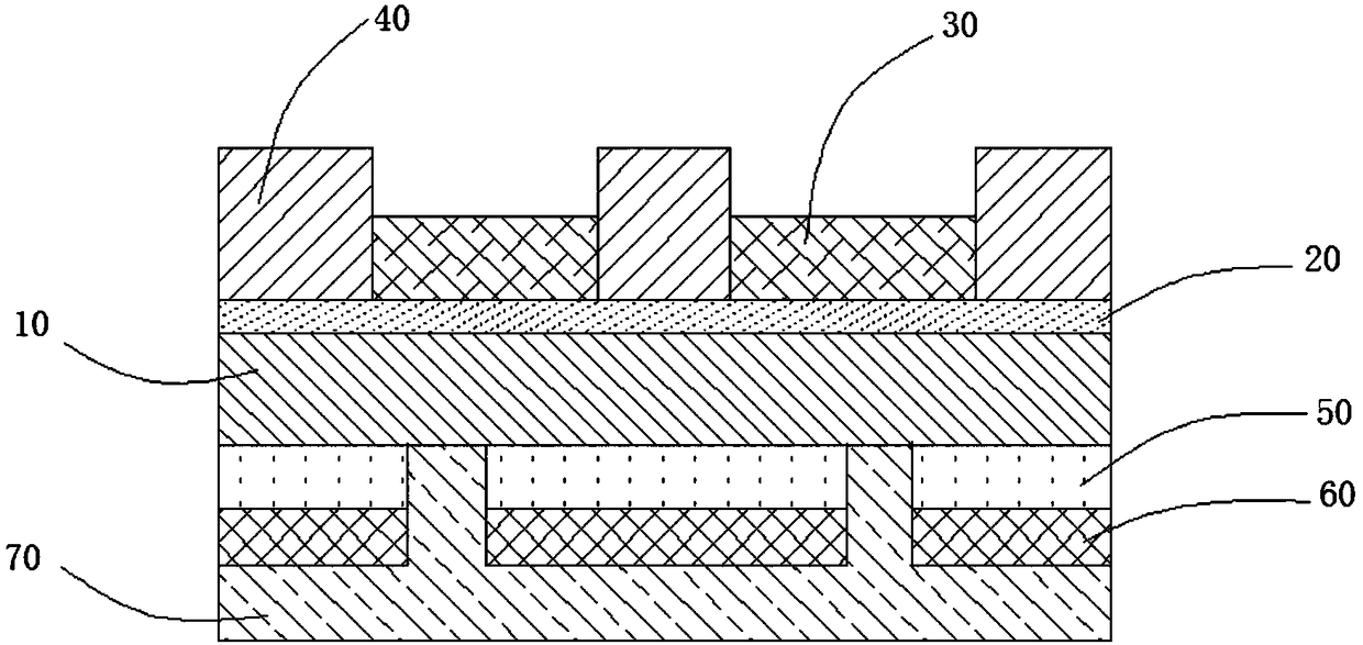
[0073] Such as figure 1 As shown, this embodiment is a rear passivated solar cell, which includes the following parts:
[0074] 1) P-type silicon wafer 10: resistivity 2Ω·cm, as an absorbing layer, converts photons that meet the conditions into electrons, and the size of the P-type silicon wafer is 2×2cm 2 ;
[0075] 2) n+ diffusion layer 20: also known as the emitter, the main function is to form a p-n junction with p-Si to selectively transport electrons, with a depth of about 0.5 μm, using POCl 3 As a phosphorus source, it is prepared by diffusion in a tube furnace;
[0076] 3) Silicon nitride anti-reflection film 30: deposited by PECVD, with a thickness of about 75nm;
[0077] 4) Negative electrode 40: obtained by screen printing and high-temperature sintering;
[0078] 5) High work function semiconductor material layer 50: obtained by thermal evaporation, its function is: through the difference in work function, a p+ layer is introduced into the Si material to indirec...
Embodiment 2
[0083] This embodiment is a back passivated solar cell. Compared with Embodiment 1, the difference lies in that the high work function semiconductor material layer is different. The high work function semiconductor material layer in the present embodiment is 9nm-V 2 o 5 / 3nm-WO 3 , other parts are the same as in Example 1.
Embodiment 3
[0085] This embodiment is a back passivated solar cell. Compared with Embodiment 1, the difference lies in that the high work function semiconductor material layer is different. The high work function semiconductor material layer in the present embodiment is 9nm-V 2 o 5 / 6nm-WO 3 , other parts are the same as in Example 1.
PUM
| Property | Measurement | Unit |
|---|---|---|
| Work function | aaaaa | aaaaa |
| Thickness | aaaaa | aaaaa |
| Thickness | aaaaa | aaaaa |
Abstract
Description
Claims
Application Information

