OLED device and manufacturing method thereof, and display apparatus

A manufacturing method and technology of a display device, which are applied in the manufacturing of semiconductor/solid-state devices, electric solid-state devices, semiconductor devices, etc., can solve the problems of restricting the application of OLED display technology, unavoidable strong reflection characteristics, and increase in device voltage, and achieve an increase in The effect of light emitting rate and light emitting uniformity, improving color rendering and reducing working voltage

Inactive Publication Date: 2018-08-31
BOE TECH GRP CO LTD
View PDF4 Cites 5 Cited by
  • Summary
  • Abstract
  • Description
  • Claims
  • Application Information

AI Technical Summary

Problems solved by technology

Usually charge generation layer (charge generation layer, CGL) is used as a connection layer to connect multiple light-emitting unit devices in series. Compared with devices with a single light-emitting unit, the current efficiency and luminous brightness of the series-connected devices can be doubled, but this kind of The cathode used in the device is a metal thin film, and the strong reflection characteristics of the metal will inevitably produce a strong microcavity effect, which seriously affects the light extraction efficiency and color rendering of the device. The light output of the bottom-emitting OLED device is as follows: figure 1 shown
More importantly, due to the preparation of multiple light-emitting units in OLEDs with a tandem structure, a charge generation layer needs to be introduced into the device as an internal electrode of the device, but this will lead to an increase in the voltage of the device and an increase in power consumption of the device, which severely limits Application of OLED display technology in the field of microdisplay

Method used


Image

  • OLED device and manufacturing method thereof, and display apparatus
  • OLED device and manufacturing method thereof, and display apparatus
  • OLED device and manufacturing method thereof, and display apparatus

Examples


Embodiment 1

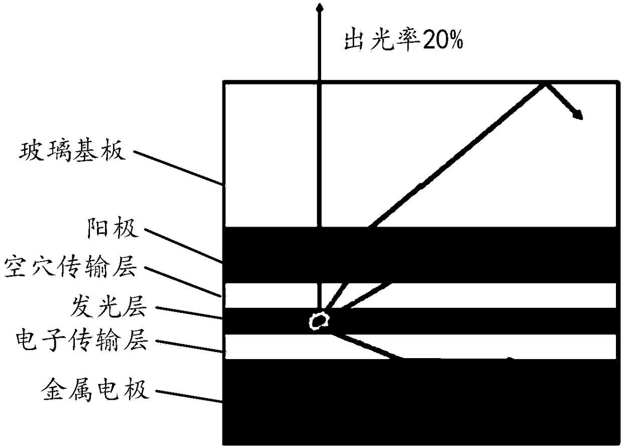
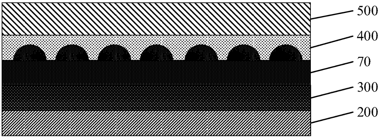
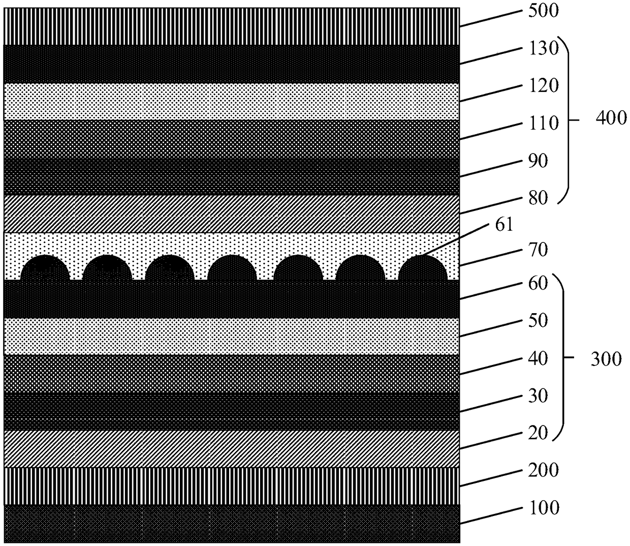
[0052] In this embodiment, the organic light-emitting layer includes: a hole injection layer, a hole transport layer, a light-emitting layer, an electron transport layer, and an electron injection layer. The OLED device includes two groups of organic light emitting layers, and the first organic light emitting layer 300 includes: a hole injection layer 20 laminated on the anode 200, a hole transport layer 30, a light emitting layer 40, an electron transport layer 50, an electron injection layer layer 60; the second organic light-emitting layer 400 includes: a second hole injection layer 80, a second hole transport layer 90, a second light-emitting layer 110, and a second electron transport layer 120 stacked on the charge generation layer , the second electron injection layer 130 .

[0053] The structural representation of the OLED device that this embodiment provides is as follows image 3 As shown, the OLED device includes: a stacked anode 200, a hole injection layer 20, a ho...

Embodiment 2

[0077] In this embodiment, the organic light-emitting layer includes: a hole injection layer, a hole transport layer, a light-emitting layer, an electron transport layer, and an electron injection layer. The OLED device includes two groups of organic light emitting layers, and the first organic light emitting layer 300 includes: a hole injection layer 20 laminated on the anode 200, a hole transport layer 30, a light emitting layer 40, an electron transport layer 50, an electron injection layer layer 60; the second organic light-emitting layer 400 includes: a second hole injection layer 80, a second hole transport layer 90, a second light-emitting layer 110, and a second electron transport layer 120 stacked on the charge generation layer , the second electron injection layer 130 .

[0078] The structural representation of the OLED device that this embodiment provides is as follows Figure 7 As shown, the OLED device includes: a base substrate 100, an anode 200, a hole injectio...

Embodiment 3

[0090] In this embodiment, the organic light-emitting layer includes: a hole injection layer, a hole transport layer, a light-emitting layer, an electron transport layer, and an electron injection layer. The OLED device includes two groups of organic light emitting layers, and the first organic light emitting layer 300 includes: a hole injection layer 20 laminated on the anode 200, a hole transport layer 30, a light emitting layer 40, an electron transport layer 50, an electron injection layer layer 60; the second organic light-emitting layer 400 includes: a second hole injection layer 80, a second hole transport layer 90, a second light-emitting layer 110, and a second electron transport layer 120 stacked on the charge generation layer , the second electron injection layer 130 .

[0091] An embodiment of the present invention provides an OLED device, and its structural schematic diagram is as follows Figure 9 As shown, it includes: a base substrate 100, a hole injection lay...


PUM


Abstract

The invention relates to the technical field of organic light emitting display, particularly relates to an OLED device and a manufacturing method thereof, and a display apparatus. The OLED device comprises a positive electrode, a negative electrode and at least two organic light emitting layers arranged between the positive electrode and the negative electrode; a charge generation layer is arranged between two adjacent organic light emitting layers; and a micro structure is arranged on at least one of the two surfaces, adjacent to the two organic light emitting layers, of the charge generationlayer. By virtue of the scheme provided by the invention, the contact area between the charge generation layer and an adjacent functional layer is enlarged, and the effective areas of the generated charges and injected charges of the charge generation layer are enlarged, so that charge generation and transmission capability of the charge generation layer is further improved, and the working voltage of the device is lowered effectively.

Description

technical field [0001] The invention relates to the technical field of organic light-emitting display, in particular to an OLED device, a manufacturing method thereof, and a display device. Background technique [0002] OLED (Organic Light Emitting Diodes, organic electroluminescent device) has many advantages such as self-luminescence, wide viewing angle, light weight, wide temperature range, large area, full curing, flexibility, low power consumption, fast response speed and low manufacturing cost. Advantages, it has important applications in the field of display and lighting, so it has attracted extensive attention from academia and industry. [0003] In order to achieve high PPI (Pixels Per Inch, pixels per inch) display, the existing technology stacks multiple independent light-emitting units, so that the same size of current flows through multiple different light-emitting units to emit light together to improve the luminous brightness With efficiency, a tandem OLED is...

Claims


Application Information

Patent Timeline
Patent Type & Authority Applications(China)
IPC IPC(8): H01L51/52H01L51/56H01L51/50H01L27/32
CPCH10K59/00H10K50/00H10K50/80H10K71/00H10K50/19H10K2102/351H10K50/854H10K2102/3026
Inventor 黄清雨焦志强闫华杰刘晓云
Owner BOE TECH GRP CO LTD
Why Eureka
Try Eureka