Optical fiber device integrated with polymer micro-nano structure in optical fiber and preparation method thereof

A technology of micro-nano structure and optical fiber device, which is applied in the direction of cladding optical fiber, optical element, optical waveguide and light guide, etc., and can solve the problems that the integration of complex polymer functional microstructure and optical fiber cannot be realized.

Active Publication Date: 2018-09-04
SHENZHEN UNIV
View PDF7 Cites 7 Cited by
  • Summary
  • Abstract
  • Description
  • Claims
  • Application Information

AI Technical Summary

Problems solved by technology

[0004] The main purpose of the present invention is to provide an optical fiber device with integrated polymer micro-nano structure in an optical fiber and its preparation method, which is used to solve the technical problem that the prior art cannot realize the integration of complex polymer functional microstructures and optical fibers

Method used


Image

  • Optical fiber device integrated with polymer micro-nano structure in optical fiber and preparation method thereof
  • Optical fiber device integrated with polymer micro-nano structure in optical fiber and preparation method thereof
  • Optical fiber device integrated with polymer micro-nano structure in optical fiber and preparation method thereof

Examples


Embodiment Construction

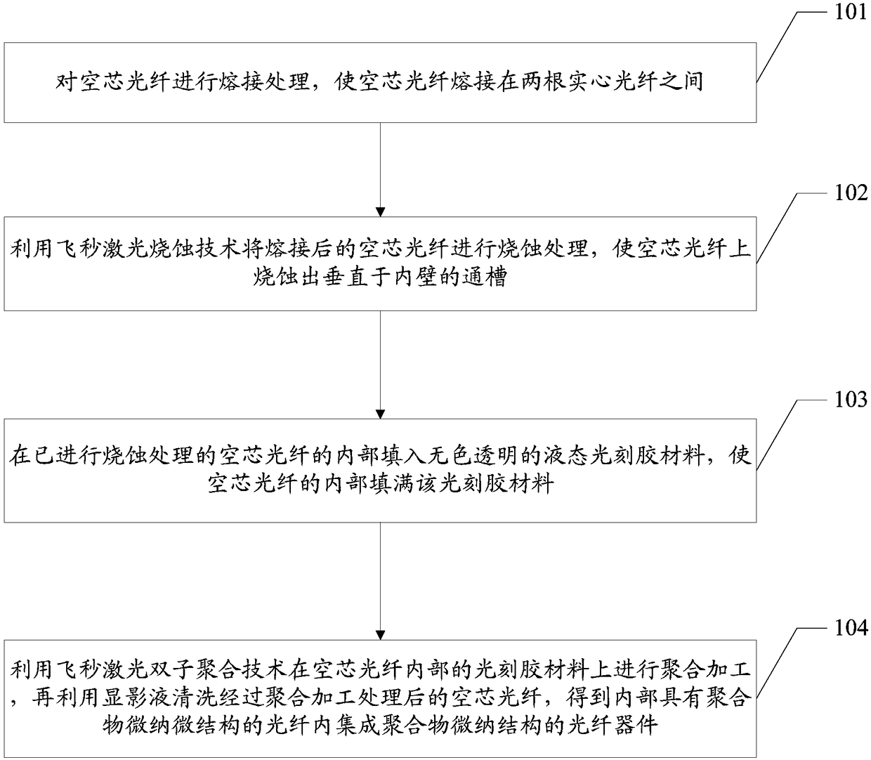
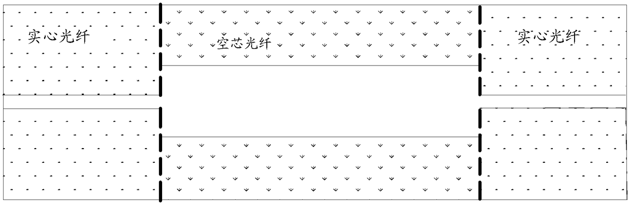
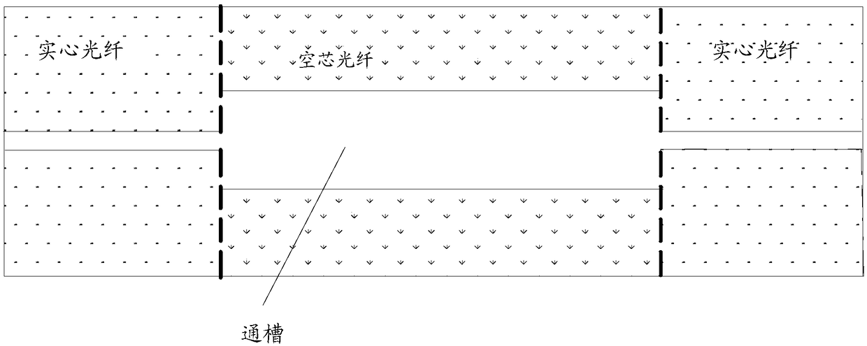
[0028] In order to make the purpose, features and advantages of the present invention more obvious and understandable, the technical solutions in the embodiments of the present invention will be clearly and completely described below in conjunction with the accompanying drawings in the embodiments of the present invention. Obviously, the described The embodiments are only some of the embodiments of the present invention, but not all of them. Based on the embodiments of the present invention, all other embodiments obtained by those skilled in the art without making creative efforts belong to the protection scope of the present invention.

[0029] Due to the technical problem that the integration of complex polymer functional microstructures and optical fibers cannot be realized in the prior art. In order to solve the above-mentioned technical problems, the present invention proposes a preparation method of an optical fiber device integrating polymer micro-nano structures in an ...


PUM


Abstract

The invention discloses a preparation method of an optical fiber device integrated with a polymer micro-nano structure in an optical fiber. The preparation method comprises the following steps: carrying out fusion welding treatment on a hollow optical fiber, so that the hollow optical fiber is fused and welded between two solid optical fibers; carrying out ablation treatment on the hollow opticalfiber subjected to fusing and welding by utilizing a femtosecond laser ablation technology, so that a through slot vertical to the inner wall is ablated on the hollow optical fiber; then filling the interior of the hollow optical fiber with a colorless and transparent photoresist material, so that the interior of the hollow optical fiber is filled with the photoresist material; then carrying out polymerization processing on the photoresist material inside the hollow optical fiber by utilizing a femtosecond laser gemini polymerization technology, and finally cleaning the hollow optical fiber subjected to the polymerization processing with developing solution, so that a device with a polymer micro-nano structure inside is obtained. The device has the polymer micro-nano structure inside, thereby having functional characteristics of a polymer; and the device well combines material characteristics of the polymer with transmission characteristics of the optical fiber together, and the integration of a complex polymer functional microstructure and the optical fiber is realized.

Description

technical field [0001] The invention relates to the field of optical fiber sensing, in particular to an optical fiber device integrating polymer micro-nano structures in an optical fiber and a preparation method thereof. Background technique [0002] Compared with quartz, polymer materials are widely used in the field of optical fiber sensing or communication due to their very good material properties. Polymer fiber Bragg grating devices made of polymer materials have higher sensitivity and are expected to be used for temperature monitoring in living organisms. [0003] The existing methods for preparing the functional microstructure of this polymer are as follows: ion beam etching, two-photon polymerization processing and ultraviolet mask exposure method, etc., wherein ion beam etching can only be processed on a plane and The processing of complex three-dimensional structures cannot be realized, so the processed equipment is not conducive to the integration of optical fiber...

Claims


Application Information

Patent Timeline
Patent Type & Authority Applications(China)
IPC IPC(8): G02B6/02
CPCG02B6/02123Y02P40/57
Inventor 廖常锐王义平李驰徐磊
Owner SHENZHEN UNIV
Why Eureka
Try Eureka