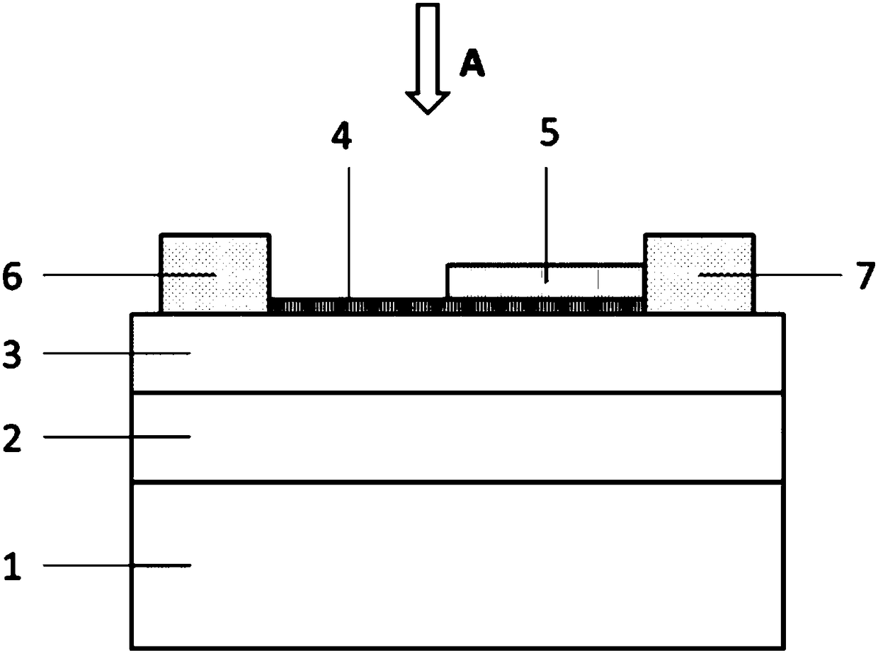
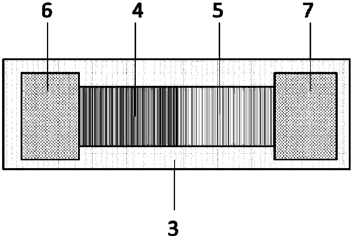
Electric field controllable 2D material Schottky diode
A Schottky diode, two-dimensional material technology, applied in circuits, electrical components, semiconductor devices, etc., can solve the problems of large parasitic resistance, complex preparation process, limited application, etc., to achieve low cost, simple method, saving occupation effect of space
- Summary
- Abstract
- Description
- Claims
- Application Information
AI Technical Summary
Problems solved by technology
Method used
Image
Examples
Embodiment 1
[0028] First, silicon is used as the substrate material, and the substrate is cleaned.
[0029] A gold thin film is grown on the substrate layer with a thickness of 100nm.
[0030] Then, a layer of PVDF-TrFE with high dielectric constant was spin-coated on the metal layer with a thickness of 50 nm.
[0031] Afterwards, a single layer of MoTe was prepared by mechanical exfoliation 2 , with a monolayer thickness of 0.7 nm. onto the PVDF-TrFE layer by a transfer technique.
[0032] Then, a layer of multilayer 2D material MoTe was prepared by mechanical exfoliation 2 , with a thickness of 2 nm. It is then transferred on the single-layer MoTe layer by transfer technology.
[0033]A 200nm-thick metal chromium film is then deposited by magnetron sputtering, and then two electrode layers are formed through a lift-off process, thus obtaining a two-dimensional material Schottky diode.
Embodiment 2
[0035] First, silicon is used as the substrate material, and the substrate is cleaned.
[0036] A gold thin film is grown on the substrate layer with a thickness of 100nm.
[0037] Then, a KDP layer with a high dielectric constant is spin-coated on the metal layer, and the thickness of the dielectric layer is 60 nm.
[0038] After that, a single layer of MoTe is directly grown on the dielectric layer by CVD method. 2 , with a monolayer thickness of 0.7 nm. Transferred onto the KDP layer by transfer technology.
[0039] Then, on the single-layer two-dimensional material layer, a layer of multi-layer two-dimensional material MoS is grown by CVD method. 2 , with a multilayer thickness of 2 nm.
[0040] Then deposit a layer of 100nm-thick metal aluminum film by electron beam evaporation, and then make metal to form two electrode layers by lift-off process, that is, obtain a two-dimensional material Schottky diode.
Embodiment 3
[0042] First, silicon is used as the substrate material, and the substrate is cleaned.
[0043] A gold thin film is grown on the substrate layer with a thickness of 80nm.
[0044] Then, deposit a layer of high dielectric constant BaTiO on the metal layer 3 layer, the thickness of the dielectric layer is 40nm.
[0045] Afterwards, a single layer of MoTe was prepared by chemical liquid phase synthesis 2 , with a monolayer thickness of 0.7 nm. transferred to the BaTiO by transfer technique 3 layer.
[0046] Then, a layer of multilayer two-dimensional material WS was prepared by chemical liquid phase synthesis 2 , the multilayer thickness is 3nm. Transferred on the single-layer two-dimensional material layer by transfer technology.
[0047] Then deposit a layer of 100nm-thick metal titanium film by thermal evaporation, and then make metal into two electrode layers through a lift-off process, that is, obtain a two-dimensional material Schottky diode.
PUM
| Property | Measurement | Unit |
|---|---|---|
| thickness | aaaaa | aaaaa |
| thickness | aaaaa | aaaaa |
| thickness | aaaaa | aaaaa |
Abstract
Description
Claims
Application Information

