PEN flexible substrate transparent thin film transistor and preparation method thereof

A transparent film and flexible substrate technology, applied in the direction of transistors, semiconductor/solid-state device manufacturing, semiconductor devices, etc., can solve the problems of high cost, toxicity, cost factors and environmental protection factors of element indium, and achieve abundant resources and simplified process The effect of the process

Inactive Publication Date: 2018-09-07
SOUTH CHINA UNIV OF TECH
View PDF3 Cites 2 Cited by
  • Summary
  • Abstract
  • Description
  • Claims
  • Application Information

AI Technical Summary

Problems solved by technology

[0003] Although the above-mentioned technologies can prepare thin films with certain transparency and low resistivity, they require annealing treatment and cannot be applied to flexible displays, and the element indium contained in materials such as ITO and IZO is costly and toxic. Will be hindered by cost factors and environmental factors

Method used


Image

  • PEN flexible substrate transparent thin film transistor and preparation method thereof
  • PEN flexible substrate transparent thin film transistor and preparation method thereof
  • PEN flexible substrate transparent thin film transistor and preparation method thereof

Examples


Embodiment

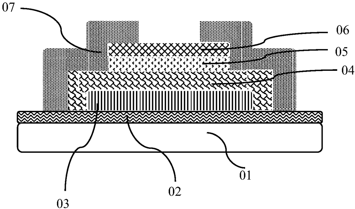
[0036] A transparent thin film transistor with a PEN flexible substrate in this embodiment, the schematic diagram of its stacked structure is as follows figure 1 shown. The glass substrate 01, flexible PEN substrate 02, AZO gate 03, Al 2 o 3 Gate insulating layer 04, IGZO semiconductor layer 05, Al 2 o 3 The semiconductor modification layer 06 and the AZO source and drain electrodes 07 are formed. The transparent thin film transistor is prepared by the following method:

[0037] (1) The glass substrate was ultrasonically cleaned with deionized water and isopropanol for about 10 minutes, and the cleaned glass substrate was placed in an oven and dried at 80-85°C.

[0038] (2) A layer of PEN flexible substrate is pasted on the cleaned and dried glass substrate with OCA glue.

[0039] (3) AZO gates of 70nm to 100nm were prepared on a PEN flexible substrate by radio frequency magnetron sputtering deposition, and the deposition process parameters were as follows: sputtering po...


PUM

PropertyMeasurementUnit
thicknessaaaaaaaaaa
thicknessaaaaaaaaaa
thicknessaaaaaaaaaa

Abstract

The invention belongs to the field of display devices, and discloses a PEN flexible substrate transparent thin film transistor and a preparation method thereof. The preparation method comprises the following steps: a glass substrate is cleaned and dried; and then a layer of PEN is coated with OCA glue; an AZO grid is prepared on the PEN layer by using radio frequency magnetron sputtering deposition; a Al2O3 grid insulating layer is prepared on the AZO grid by using the radio frequency magnetron sputtering deposition; an IGZO semiconductor layer is deposited on the grid insulating layer by using pulsed direct current magnetron sputtering; a Al2O3 semiconductor modified layer is deposited on the semiconductor layer by using the radio frequency magnetron sputtering; and AZO source and drain electrodes are deposited by using pulse laser so as to obtain a PEN flexible substrate transparent thin film transistor. According to the PEN flexible substrate transparent thin film transistor and thepreparation method in the present invention, the AZO is adopted as a grid electrode and source and drain electrodes of the TFT device, and the obtained TFT device has the advantages of high performance, high transparency, and non-toxicity.

Description

technical field [0001] The invention belongs to the field of display devices, and in particular relates to a PEN flexible substrate transparent thin film transistor and a preparation method thereof. Background technique [0002] At present, the main difficulty in preparing highly transparent and flexible thin film crystals is that the prepared electrode materials are difficult to be compatible with high transparency and high conductivity. Existing technologies to solve the above problems mainly use indium-containing materials such as ITO and IZO as electrodes of thin film transistors and perform annealing treatment. The indium element provides a large amount of electrons for the electrode film. In addition, annealing treatment can greatly improve the internal defects of the electrode, and can prepare a high-conductivity, high-transparency film ([1] Hoffman RL, Norris B J, Wager J F.ZnO-based transparent thin -film transistors[J].Applied Physics Letters,2003,82(5):733-735.[2...

Claims


Application Information

Patent Timeline
Patent Type & Authority Applications(China)
IPC IPC(8): H01L21/336H01L29/786
CPCH01L29/66742H01L29/78642
Inventor 姚日晖章红科宁洪龙李晓庆张啸尘邓宇熹邓培淼周尚雄袁炜健彭俊彪
Owner SOUTH CHINA UNIV OF TECH
Why Eureka
Try Eureka