A kind of vertical structure LED chip of double insertion layer reflector structure and preparation method thereof
A LED chip and vertical structure technology, applied in semiconductor devices, electrical components, circuits, etc., can solve problems such as poor thermal stability and poor adhesion of Ag-based reflectors
- Summary
- Abstract
- Description
- Claims
- Application Information
AI Technical Summary
Problems solved by technology
Method used
Image


Examples
Embodiment 1
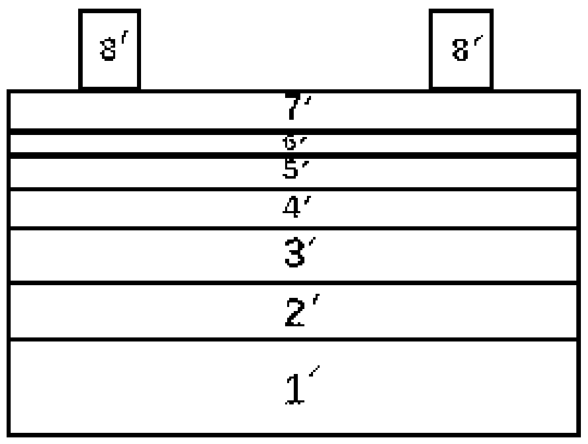
[0073] refer to Figure 3-1 , a vertical structure LED chip with double insertion layer reflector structure, its preparation method comprises,
[0074] LED epitaxial wafer growth: first epitaxially grow LED epitaxial wafer 9' on Si substrate, including n-type doped GaN film grown on Si substrate, InGaN / GaN quantum well grown on n-type doped GaN film and The p-type doped GaN thin film grown on the InGaN / GaN quantum well; the Si substrate takes the (111) plane as the epitaxial plane; the thickness of the n-type doped GaN layer is 2 μm; the InGaN / GaN quantum well 8 cycles of InGaN well layer / GaN barrier layer, wherein the thickness of InGaN is 4nm, the thickness of GaN barrier layer is 12nm; the thickness of the p-type doped GaN film is 200nm; the first step of inserting the metal layer into the growth mirror : Electron beam evaporation, magnetron sputtering or thermal evaporation equipment is used on the surface of the LED epitaxial wafer, and the first layer of the evaporation...
Embodiment 2
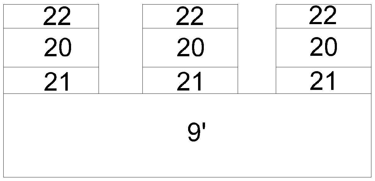
[0081] refer to Pic 4-1 , a vertical structure LED chip with double insertion layer reflector structure, its preparation method comprises,
[0082] LED epitaxial wafer growth steps: first epitaxially grow LED epitaxial wafer 9" on Si substrate, LED epitaxial wafer 9" includes n-type doped GaN thin film grown on Si substrate, n-type doped GaN thin film grown on n-type doped GaN thin film InGaN / GaN quantum wells and p-type doped GaN films grown on InGaN / GaN quantum wells; the Si substrate takes the (111) plane as the epitaxial plane; the thickness of the n-type doped GaN layer is 2 μm; The InGaN / GaN quantum well is an InGaN well layer / GaN barrier layer with 8 periods, wherein the thickness of InGaN is 4nm, and the thickness of the GaN barrier layer is 12nm; the thickness of the p-type doped GaN film is 200nm;
[0083] The step of growing the reflector first inserting the metal layer: using electron beam evaporation, magnetron sputtering or thermal evaporation equipment on the ...
Embodiment 3
[0090] A vertical structure LED chip with a double-insertion layer reflector structure, the preparation method of which comprises,
[0091] LED epitaxial wafer growth steps: first grow LED epitaxial wafers on Si substrates, LED epitaxial wafers include n-type doped GaN films grown on Si substrates, grow InGaN / GaN quantum wells on n-type doped GaN films and A p-type doped GaN thin film is grown on the InGaN / GaN quantum well; the Si substrate takes the (111) plane as an epitaxial plane; the thickness of the n-type doped GaN layer is 1 μm; the InGaN / GaN quantum well is 4 periods of InGaN well layer / GaN barrier layer, wherein the thickness of InGaN is 7nm, the thickness of GaN barrier layer is 3nm; the thickness of the p-type doped GaN film is 100nm;
[0092] The first step of inserting the metal layer of the growing reflector: using electron beam evaporation, magnetron sputtering or thermal evaporation equipment on the surface of the LED epitaxial wafer, and evaporating the first...
PUM
| Property | Measurement | Unit |
|---|---|---|
| thickness | aaaaa | aaaaa |
| thickness | aaaaa | aaaaa |
| thickness | aaaaa | aaaaa |
Abstract
Description
Claims
Application Information
 - R&D
- Intellectual Property
- Life Sciences
- Materials
- Tech Scout
- Unparalleled Data Quality
- Higher Quality Content
- 60% Fewer Hallucinations
Browse by: Latest US Patents, China's latest patents, Technical Efficacy Thesaurus, Application Domain, Technology Topic, Popular Technical Reports.
© 2025 PatSnap. All rights reserved.Legal|Privacy policy|Modern Slavery Act Transparency Statement|Sitemap|About US| Contact US: help@patsnap.com