Flexible epitaxial ferroelectric-gate thin-film transistor and preparation method thereof

A thin film transistor and ferroelectric thin film technology, applied in the field of flexible epitaxial ferroelectric gate thin film transistor and its preparation, can solve the problems of no high temperature resistance, slow reading speed, easy polarization fatigue and the like, and achieve excellent high temperature resistance performance, Overcome the effects of poor bonding, good lattice matching

Inactive Publication Date: 2018-09-18
XIANGTAN UNIV
View PDF1 Cites 2 Cited by
  • Summary
  • Abstract
  • Description
  • Claims
  • Application Information

AI Technical Summary

Problems solved by technology

Usually, the gate dielectric material commonly used in the fabrication of flexible thin film transistors is low-cost, low-temperature prepared organic ferroelectric polymers. Therefore, it is necessary to develop new high-performance inorganic ferroelectric materials.
Moreover, the existing production of flexible thin film transistors generally directly forms thin film transistors on flexible substrates, and flexible substrates are generally polyethylene terephthalate (PET), polyethylene naphthalate (PEN), polyether Sulfone resin (PES), polyimide (PI) and other materials, but because they do not have the disadvantage of high temperature resistance, they are not suitable for growing traditional ferroelectric materials that require high temperature preparation

Method used


Image

  • Flexible epitaxial ferroelectric-gate thin-film transistor and preparation method thereof
  • Flexible epitaxial ferroelectric-gate thin-film transistor and preparation method thereof
  • Flexible epitaxial ferroelectric-gate thin-film transistor and preparation method thereof

Examples


Embodiment 1

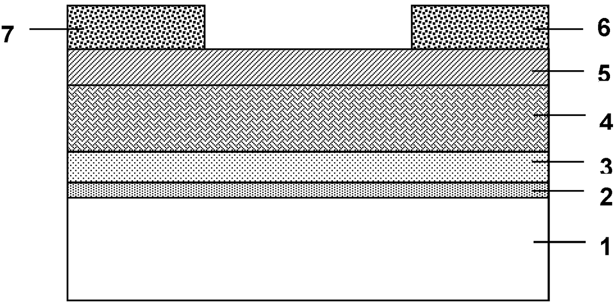
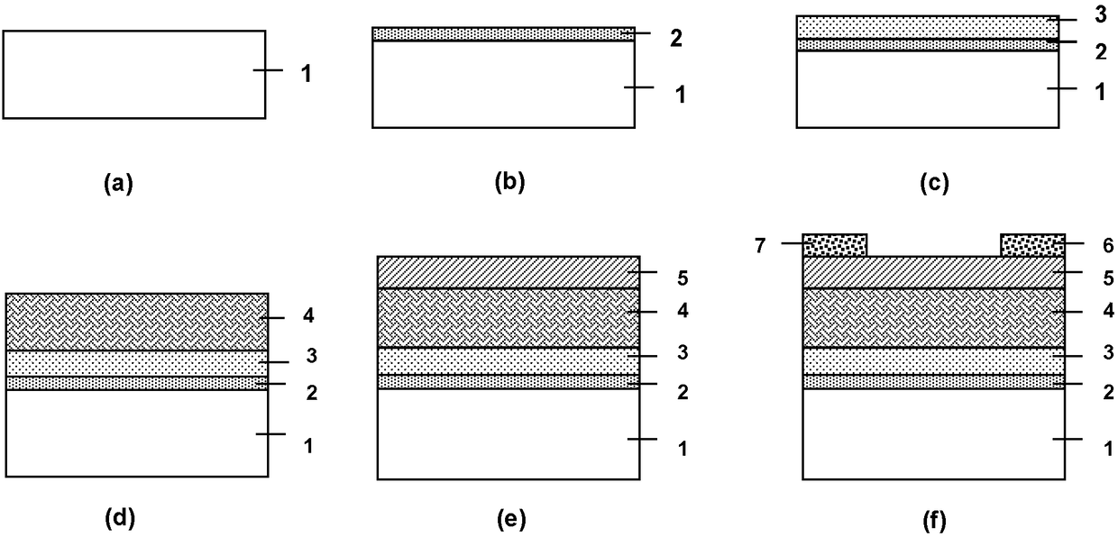
[0067] like figure 1 As shown, Embodiment 1 discloses a flexible epitaxial ferroelectric gate thin film transistor, comprising: a mica flexible substrate 1; a buffer layer 2 formed on the mica substrate 1; a bottom gate electrode 3 formed on the buffer layer 2; The epitaxial ferroelectric thin film layer 4 formed on the bottom gate electrode 3; the channel layer 5 formed on the epitaxial ferroelectric thin film layer 4; the source electrode 6 formed on the channel layer 5; The drain electrode 7 is formed by separating the source electrode.

[0068] The ferroelectric thin film layer 4 is composed of a lead zirconate titanate thin film material, and the ratio of the amounts of Pb, Zr and Ti in the lead zirconate titanate thin film material is 1:0.1:0.9; the thickness of the ferroelectric thin film layer 4 is 150 nm; 1 is composed of natural mica material with a thickness of 20 μm; the buffer layer 2 is composed of CoFe 2 O 4 It is composed of thin film material, and the thick...

Embodiment 2

[0077] Embodiment 2 discloses a flexible epitaxial ferroelectric gate thin film transistor, such as figure 1 shown, including:

[0078] Mica flexible substrate 2;

[0079] The buffer layer 2 formed on the mica substrate 1;

[0080] The bottom gate electrode 3 formed on the buffer layer 2;

[0081] an epitaxial ferroelectric thin film layer 4 formed on the bottom gate electrode 3;

[0082] The channel layer 5 formed on the epitaxial ferroelectric thin film layer 4;

[0083] The source electrode 6 formed on the channel layer 5;

[0084] and a drain electrode 7 formed on the channel layer and separated from the source electrode.

[0085] The ferroelectric thin film layer 4 is composed of a lead zirconate titanate thin film material, and the ratio of the amounts of Pb, Zr, and Ti in the lead zirconate titanate thin film material is 1:0.2:0.8; the thickness of the ferroelectric thin film layer 4 is 120 nm; Substrate 1 is composed of natural mica material with a thickness of 1...

Embodiment 3

[0094] Embodiment 3 discloses a flexible epitaxial ferroelectric gate thin film transistor, such as figure 1 shown, including:

[0095] Mica flexible substrate 2;

[0096] A buffer layer 2 formed on the mica substrate 1;

[0097] a bottom gate electrode 3 formed on the buffer layer 2;

[0098] The epitaxial ferroelectric thin film layer 4 formed on the bottom gate electrode 3;

[0099] A channel layer 5 formed on the epitaxial ferroelectric thin film layer 4;

[0100] a source electrode 6 formed on the channel layer 5;

[0101] and a drain electrode 7 formed on the channel layer and separated from the source electrode.

[0102] The ferroelectric thin film layer 4 is composed of lead zirconate titanate thin film material, the ratio of the amount of Pb, Zr, and Ti substances in the lead zirconate titanate thin film material is 1:0.3:0.7; the thickness of the ferroelectric thin film layer 4 is 180nm; Substrate 1 is composed of natural mica material with a thickness of 30 μm...


PUM

PropertyMeasurementUnit
thicknessaaaaaaaaaa
thicknessaaaaaaaaaa
thicknessaaaaaaaaaa

Abstract

The invention discloses a flexible epitaxial ferroelectric-gate thin-film transistor and a preparation method thereof. The transistor is composed of a flexible mica substrate, a buffer layer formed onthe substrate, a bottom gate electrode formed on the buffer layer, an epitaxial ferroelectric thin film layer formed on the bottom gate electrode, a channel layer formed on the epitaxial ferroelectric thin film layer, a source electrode formed on the channel layer, and a drain electrode being formed on the channel layer and being separated from the source electrode. According to the invention, the perovskite oxide SrRuO3 epitaxial film with metal conductivity is used as the bottom gate electrode and the perovskite oxide epitaxial ferroelectric film is used as a gate dielectric layer. The transistor has the excellent mechanical bending property and is resistant to bending with the 2-mm bending radius for repeated 1000 times; and the electrical property of the ferroelectric gate thin-film transistor is kept to be unchanged basically. The reading and writing speed is fast; and the high temperature-resistant performance is excellent; and after annealing at a temperature of 400 DEG C, theelectrical property of the transistor does not change obviously. Moreover, the preparation process is simple; the process is stable; and the manufacturing cycle is short.

Description

technical field [0001] The invention belongs to the technical field of ferroelectric gate thin film transistors, and particularly relates to a flexible epitaxial ferroelectric gate thin film transistor and a preparation method thereof. Background technique [0002] At present, conventional electronic devices in the microelectronics industry are usually fabricated on silicon substrates in combination with micro-nano fabrication processes. These silicon-based electronic devices played an important role in the development of human society in the second half of the last century. However, with the future needs of electronic products in terms of portability, ultra-thinness, bendability, wearability, etc., it is necessary to find A new generation of electronic devices and related fabrication techniques. Flexible electronic devices have shown a rapid development trend in recent years due to their unique ductility and their advantages in high-efficiency and low-cost manufacturing pr...

Claims


Application Information

Patent Timeline
Patent Type & Authority Applications(China)
IPC IPC(8): H01L29/786H01L21/336H01L21/02
CPCH01L21/02098H01L29/66227H01L29/786
Inventor 钟向丽任传来谭丛兵王金斌李波郭红霞宋宏甲廖敏
Owner XIANGTAN UNIV
Why Eureka
Try Eureka