Adjustable Negative Group Delay Circuit

A negative group delay and circuit technology, applied in the direction of electrical components, electrical digital data processing, instruments, etc., can solve the problems of narrow adjustment range, increased insertion loss, limitation, etc., and achieve simple implementation method, wide application frequency band, insertion low loss effect

Active Publication Date: 2021-08-10
10TH RES INST OF CETC
View PDF0 Cites 0 Cited by
  • Summary
  • Abstract
  • Description
  • Claims
  • Application Information

AI Technical Summary

Problems solved by technology

Although this structure can adjust the center frequency and negative group delay at the same time, its adjustment range is relatively narrow, and the lumped resistance used leads to increased insertion loss, which can reach as high as 20dB
In order to improve the return loss, an "electrically adjustable negative group delay circuit with stable insertion loss" is proposed in the prior art, which adopts an adjustable negative group delay circuit with input / output impedance matching and impedance converter, and uses Varactor diodes are used to adjust the negative group delay value. The disadvantage is that the structure is slightly complicated, an additional active bias circuit is required, and only adjustable negative group delay can be achieved.
Limited by the use of lumped components, both of the above two circuits require input and output matching circuits, which increases the resources and difficulty of design, and the application in high frequency bands greater than 10GHz is also limited

Method used


Image

  • Adjustable Negative Group Delay Circuit
  • Adjustable Negative Group Delay Circuit
  • Adjustable Negative Group Delay Circuit

Examples


Embodiment Construction

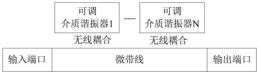
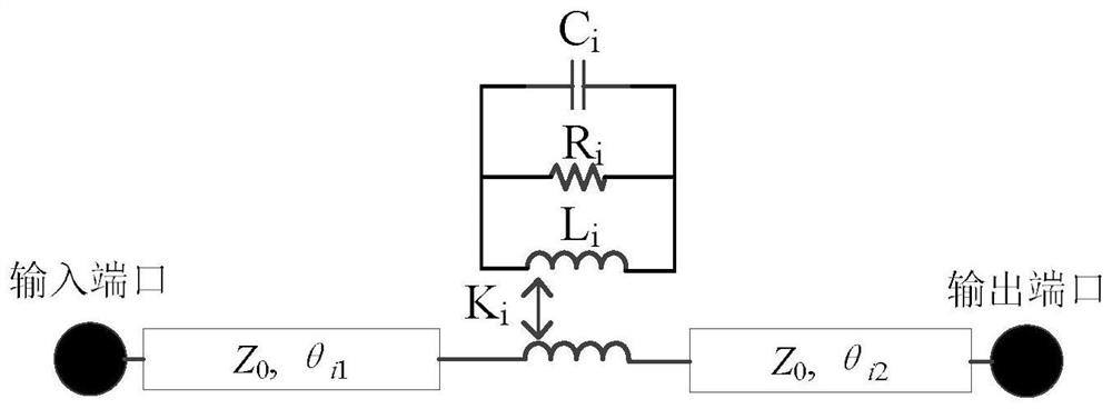
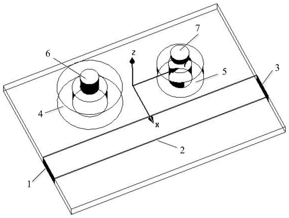
[0020] refer to figure 1 . In the embodiment described below, an adjustable negative group delay circuit includes: an input port, a section of microstrip line, N adjustable dielectric resonators (N is an integer and N≥1), and an output port, wherein : The input port is connected to the input port of the microstrip line, and the output port is connected to the output port of the microstrip line. Any adjustable dielectric resonator i (1≤i≤N) among the N adjustable dielectric resonators has adjustable resonant frequency and unloaded quality factor, and is located next to the microstrip line. The tunable dielectric resonator i works in the transverse electric wave TE mode, and is connected to the microstrip line through wireless coupling. The impedance of the input port and the impedance of the output port are the same as the impedance of the microstrip line. The wireless coupling method includes but not limited to magnetic force line coupling.

[0021] The adjustable dielectr...


PUM


Abstract

The invention discloses an adjustable negative group delay circuit, aiming to provide a negative group delay circuit with simple structure, low circuit insertion loss and no need for input and output matching circuits. The adjustable negative group delay circuit of the present invention includes: a section of microstrip line connected in series between the input port and the output port and N dielectric resonators with adjustable resonant frequency and unloaded quality factor, wherein: N adjustable dielectric resonators The resonator is equivalent to N different parallel RLC resonant circuits, which are located next to the microstrip line and fixed on the same printed board as the microstrip line; N dielectric resonators work in the transverse wave TE mode and are connected to the microstrip through wireless coupling. After the strip line is coupled with the microstrip line, N-band negative group delay is generated near the resonant frequency of N dielectric resonators; the input port impedance and output port impedance of the adjustable negative group delay circuit are the same as the microstrip line impedance. The invention can be widely used in technical fields requiring negative group delay and adjustable negative group delay.

Description

technical field [0001] The invention relates to a negative group delay circuit that can be applied in technical fields such as radio frequency microwave circuits, communication, navigation, measurement, radar, etc., especially an adjustable negative group delay circuit of a microstrip coupling dielectric resonator. Background technique [0002] Group delay is a very important parameter used to represent the phase linearity of a signal in a transmission system, especially in the field of radio frequency and microwave. Group delay specifically refers to the delay generated by the overall signal when the group signal passes through the transmission system or transmission network. It emphasizes the transmission time of the overall envelope of the signal, so it is sometimes called envelope delay. In recent years, the phenomenon of negative group delay has been realized in electronic circuits, and has been widely used in various communication systems, feedforward amplifiers, anten...

Claims


Application Information

Patent Timeline
Patent Type & Authority Patents(China)
IPC IPC(8): H03H7/32G06F30/3308
CPCG06F30/367H03H7/325
Inventor 陈文兵
Owner 10TH RES INST OF CETC
Why Eureka
Try Eureka