

Method for optimizing performance of vanadium oxide thin film through low valent vanadium seed layer
A technology of vanadium oxide thin film and seed layer, applied in coating, ion implantation plating, metal material coating process, etc., can solve the problems of poor film performance and complex process, achieve low preparation temperature, good process compatibility, Effect of annealing temperature reduction
- Summary
- Abstract
- Description
- Claims
- Application Information
AI Technical Summary
Problems solved by technology
Method used
Image

Examples
Embodiment 1
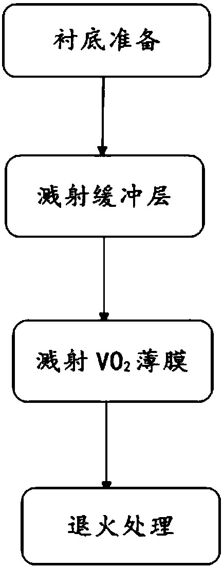
[0034] Such as figure 1 As shown, the method for optimizing the performance of the vanadium oxide thin film using a low-valent vanadium seed layer provided in this embodiment includes the following steps:
[0035] (1) Using Al 2 o 3 Substrate: Al 2 o 3 Put the substrate in acetone for 30 minutes to remove surface impurities, then put it in absolute ethanol for 30 minutes to remove residual acetone, and finally put it in absolute ethanol for storage. 2 blow dry;
[0036] (2) Using magnetron sputtering technology on Al 2 o 3 The vanadium oxide thin film is prepared on the substrate, and the specific process conditions are:
[0037] Target material: metal vanadium target; background vacuum degree: less than 2×10 -3 Pa; Sputtering temperature: 60±1°C; Ar flow rate during sputtering: 98 sccm; O during the first sputtering process 2 Flow rate: 0.5sccm, the first sputtering time is 1min; during the second sputtering process, O 2 Flow rate: 1sccm, the second sputtering time ...
Embodiment 2
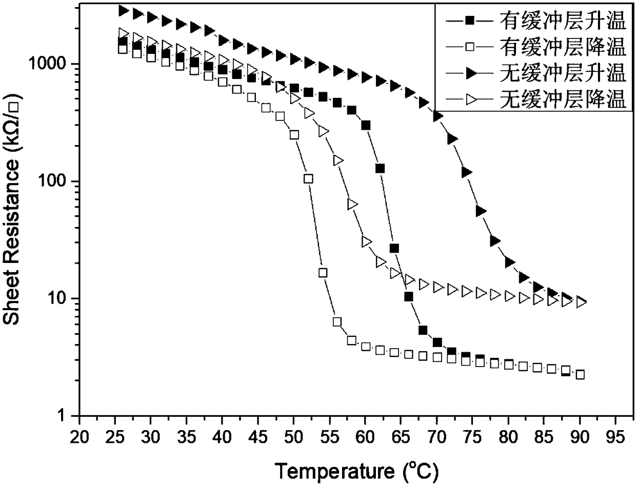
[0042] Other conditions remain the same, and the first sputtering process of (2) in 1 will be implemented in detail. 2 The flow rate is changed to: 0.4sccm, the phase transition amplitude of the prepared vanadium oxide film is 464 times, the loop width is 8.63°C, and the phase transition temperature is 60°C. Although the phase transition amplitude is lower than that of the film under the condition of 0.5sccm, but The loop width and the phase transition temperature are both smaller, indicating that the performance of the vanadium oxide film can be adjusted by changing the ratio of argon to oxygen for making the seed layer.
[0043] Such as image 3 Shown is the graph of the square resistance temperature characteristic curve of the vanadium oxide thin film prepared in this embodiment.
Embodiment 3
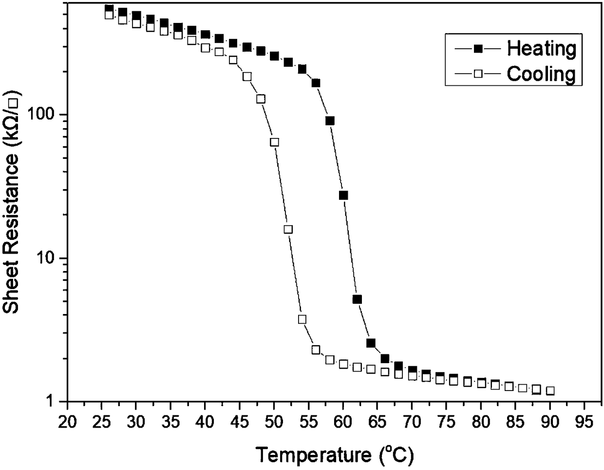
[0045] Other conditions remain unchanged, the first sputtering time in (2) in the specific embodiment one is changed to: 2min, the phase transition amplitude of the prepared vanadium oxide film is 423 times, the loop width is 5.37°C, and the phase transition temperature is 55.88°C ℃. Although the phase transition amplitude is not as large as before, the loop width and phase transition temperature are further reduced, indicating that adjusting the thickness of the seed layer can change the properties of the vanadium oxide film.
[0046] Such as Figure 4 Shown is the graph of the square resistance temperature characteristic curve of the vanadium oxide thin film prepared in this embodiment.
PUM
| Property | Measurement | Unit |
|---|---|---|
| phase transition temperature | aaaaa | aaaaa |
| phase transition temperature | aaaaa | aaaaa |
Abstract
Description
Claims
Application Information